
Integration Guide


2:Description and Specifications
MatchPort b/g Pro Integration Guide 23
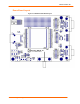
Recommended PCB Layout
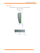
The hole pattern and mounting dimensions for the MatchPort b/g Pro device server are
shown in the following drawing:
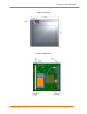
Figure 2-14. PCB Layout (Top View)
Note: If a socket is used for product development purpose only, two 2-mm, 20-pin sockets
spaced 1.42" apart can be used (e.g., Samtec P/N SMM-120-02-S-S-TR).
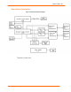
u To optimize noise and cross-talk reduction, noise immunity, and impedance
matching on ETX+, ETX-, ERX+, ERX-, follow these guidelines when routing
traces on the target PCB:
- Route (ETX+, ETX-) pair as close to each other as possible, and far away
from ERX+, ERX- and other signals
- Route (ERX+, ERX-) pair as close to each other as possible, and far away
from ETX+, ETX- and other signals
- Set up PCB routing properties on each pair (ETX+, ETX-) and (ERX+, ERX-)
to achieve 100-ohm impedance.
- For EMI purposes, connect the metal housing (shield) of the RJ45 jack to
Power Ground or Earth Ground and do not allow floating.
If power ground and earth ground are to be separated, add ceramic
capacitors in the range of 1000 pF to 0.1 uF in a stitching pattern between
the two grounds to provide low impedance paths at high frequencies. The
voltage rating on the ceramic capacitors should be much higher than the
required isolation voltage between the two grounds.
u Connect 3.3V and ground on the MatchPort b/g Pro directly to 3.3V power and
ground planes of the target board in place of heavy trace routing. This will
minimize noises as well as voltage drops due to the trace.
u Make the RESETIN# trace on the target board as short as possible to avoid reset
occurrences when transient voltages such as those caused by ESD are present.