
Product Info

LPWA M
odule Series
BG95 Series Hardware Design
BG95_S
eries_Hardware_Design 33 / 106
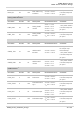
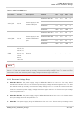
Pin N
ame Pin No. I/O Description DC Characteristics Comment
ADC
0 24 AI
General-purpose
ADC interface
Voltage range:
0.1–1.8 V
Do not use ADC0
and ADC1
simultaneously.
If unused, keep
these pins open.
ADC
1 2 AI
General-purpose
ADC interface
Voltage range:
0.1–1.8 V
Ot
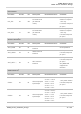
her Interface Pins
Pin Name Pin No. I/O Description DC Characteristics Comment
W
_DISABLE#*
18 DI
Ai
rplane mode
control
V
IL
min = -0.3 V
V
I
L
m
ax = 0.6 V
V
I
H
min = 1.2 V
V
IH
m
ax = 2.0 V
1.8 V power domain.
Pulled up by default.
When it is in low
voltage level, the
module can enter
airplane mode.
If unused, keep this
pin open.
AP_R
EADY* 19 DI
Application
processor sleep
state detection
V
I
L
m
in = -0.3 V
V
I
L
m
ax = 0.6 V
V
I
H
m
in = 1.2 V
V
I
H
m
ax = 2.0 V
1.8 V power domain.
If unus
ed, keep this
pin open.
USB_
BOOT 75 DI
Force the
module into
emergency
download mode
V
I
L
m
in = -0.3 V
V
I
L
m
ax = 0.6 V
V
IH
m
in = 1.2 V
V
I
H
max = 2.0 V
1.8 V power domain.
If unus
ed, keep this
pin open.
PON
_TRIG 96 DI
Wake up the
module from
PSM
1.8 V power domain.
Risi
ng-edge
triggered.
Pulled-down by
default.
If unused, keep this
pin open.
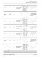
GRF
C Interfaces
Pin N
ame Pin No. I/O Description DC Characteristics
Com
ment
GRFC1
3)
83 DO
Gener
ic RF
controller
V
OL
max = 0.45 V
V
OH
min =
1.35 V
1.8 V power domain.
If unus
ed, keep this
pin open.
GRFC2
3)
84 DO
Gener
ic RF
controller
V
OL
m
ax = 0.45 V
V
OH
min =
1.35 V
BOOT_CONFIG.
Do not pull it up
before startup.
1.8 V power domain.