
Product Info

LP
WA Module Series
BG95 Series Hardware Design
BG95_S
eries_Hardware_Design 34 / 106
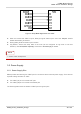
1.
1)
Only
BG95-MF supports ANT_WIFI (pin 56)
.
2.
2)
BG95-MF
does not support GPIO3 and GPIO4 interfaces (pin 64 and pin 65).
3.
3)
BG95-M4 does not support GRFC interfaces (pin 83 and pin 84).
4. For
every VBAT transition/re-insertion from 0 V, the minimum power supply voltage should be higher
than 2.7 V. After the module starts up normally, the minimum safety voltage is 2.6 V. In order to
ensure
full-function mode, the minimum power supply voltage should be higher than 2.8 V.
5. P
WRKEY output voltage is 1.5 V because of the voltage drop inside the Qualcomm chipset. Due to
pl
atform limitations, the chipset has integrated the reset function into PWRKEY. Therefore, never pull
down
PWRKEY to GND permanently.
6. RES
ET_N connects directly to PWRKEY inside the module.
7. Do
not use ADC0 and ADC1 simultaneously, as ADC1 connects directly to ADC0 inside the module.
BG95 s
eries module supports use of only one ADC interface at a time: either ADC0 or ADC1.
8. W
hen PSM is enabled, the function of PSM_IND pin will be activated after the module is reboote
d.
When PSM_IND is in high voltage level, the module is in normal operation state, when it is in low
v
oltage level, the module is in PSM.
9. GNSS_TXD (pin 27) and GRFC2 (pin 84) are BOOT_CONFIG pins. Never pull them up before
star
tup, otherwise the module cannot power on normally.
10. Kee
p all RESERVED pins and unused pins open.
11. “*
” means under development.
3.3. Op
erating Modes
The t
able below briefly summarizes the various operating modes of BG95 series module.
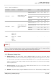
If unused, keep this
pin open.
RES
ERVED Pins
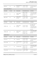
Pin Name Pin No. I/O Description DC Characteristics
Comment
RESERVED
11–14, 16,
51, 57, 63,
76–78,
92–95,
97–99
Reserved
Keep these pins
open.
NOT
ES