
Product Info


LP
WA Module Series
BG95 Series Hardware Design
BG95_S
eries_Hardware_Design 49 / 106
For
more details about USB 2.0 specification, please visit https://www.usb.org/.
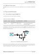
The USB interface is recommended to be reserved for firmware upgrade in application designs. The
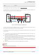
following figure shows a reference design of USB interface.
Figure 16: Reference Design of USB Interface
In order to ensure the integrity of USB data line signal, components R1 and R2 should be placed close to
the module. The extra stubs of trace must be as short as possible.
The following principles should be complied with while designing the USB interface, so as to meet USB
2.0 specification.
It is important to route the USB signal traces as differential pairs with ground surrounded. The
impedance of USB differential trace is 90 Ω.
Do not route signal traces under crystals, oscillators, magnetic devices and RF signal traces. It is
important to route the USB differential traces in inner-layer of the PCB, and surround the traces with
ground on that layer and with ground planes above and below.
Junction capacitance of the ESD protection device might cause influences on USB data lines, so
please pay attention to the selection of the device. Typically, the stray capacitance should be
less
than 2 pF.
Keep the ESD protection devices
as cl
ose to the USB connector as possible.
BG95 c
an only be used as a slave device.
GN
D 3 Ground
NOT
E