
Product Info

LP
WA Module Series
BG95 Series Hardware Design
BG95_S
eries_Hardware_Design 51 / 106
Tab
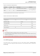
le 14: Pin Definition of Debug UART Interface
Table 15: Pin Definition of GNSS UART Interface
GNS
S_TXD is a BOOT_CONFIG pin. Never pull it up before startup, otherwise the module cannot power
on nor
mally.
The l
ogic levels of UART interfaces are described in the following table.
Table 16: Logic Levels of Digital I/O
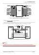
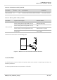
The module provides 1.8 V UART interfaces. A voltage-level translator should be used if customers’
application is equipped with a 3.3 V UART interface. The voltage-level translator TXS0108EPWR
provided by Texas Instruments is recommended. The following figure shows a reference design of the
main UART interface.
Pin N
ame
Pin N
o.
I/
O
De
scription
Comme
nt
DB
G_RXD 22 DI Debug UART receive 1.8 V power domain
DB
G_TXD 23 DO Debug UART transmit 1.8 V power domain
Pin N
ame
Pin N
o.
I/
O
De
scription
Com
ment
GNS
S_TXD 27 DO GNSS UART transmit
BOOT_CONFIG.
Do not pull it up before startup.
1.8 V power domain
GNSS_RXD 28 DI GNSS UART receive 1.8 V power domain
Param
eter
M
in.
M
ax.
Un
it
V
IL
-0.3 0.6 V
V
IH
1.2 2.0 V
V
OL
0 0.45 V
V
OH
1.35 1.8 V
NOT
E