
Product Info

LP
WA Module Series
BG95 Series Hardware Design
BG95_S
eries_Hardware_Design 53 / 106
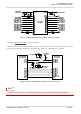
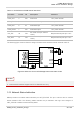
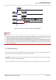
Figur
e 19: Reference Circuit with Dual-Transistor Circuit (Recommended for GNSS UART)
GNS
S_TXD is a BOOT_CONFIG pin (pin 27), therefore voltage-level translation IC solution with pull-up
circu
it or signal transistor/MOSFET circuit is not applicable to it. The dual-transistor circuit solution is
reco
mmended for GNSS UART.
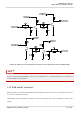
3.12. PCM and I2C Interfaces*
BG95 prov
ides one Pulse Code Modulation (PCM) digital interface and one I2C interface which are used
for VoLTE or GSM CS voice only.
The following table shows the pin definition of the two interfaces which can be applied on audio codec
design.
NOT
E