
Product Info

LP
WA Module Series
BG95 Series Hardware Design
BG95_S
eries_Hardware_Design 59 / 106
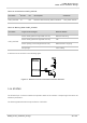
Tab
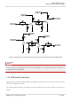
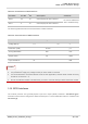
le 23: Pin Definition of ADC Interface
Pin Name Pin No. I/O Description Comment
ADC
0 24 AI General-purpose ADC interface
Do not use ADC0 and
ADC1 simultaneously.
ADC1 2 AI General-purpose ADC interface
The
following table describes the characteristics of ADC interfaces.
Table 24: Characteristics of ADC Interfaces
1. ADC input voltage must not exceed 1.8 V.
2. It
is prohibited to supply any voltage to ADC pin when VBAT is removed.
3. It
is recommended to use resistor divider circuit for ADC application, and the divider resistor accuracy
shou
ld be no less than 1 %.
4. Do
not use ADC0 and ADC1 simultaneously, as ADC1 connects directly to ADC0 inside the module.
3.18. GPIO
Interfaces
The
module provides nine general-purpose input and output (GPIO) interfaces. AT+QCFG="gpio"
command can be used to configure the status of GPIO pins. For more details about the AT command, see
document [2].
Param
eter
M
in.
Ty
p.
M
ax.
Un
it
Vo
ltage Range 0.1 1.8 V
Re
solution (LSB) 64.979 μV
Analog Bandwidth 500 kHz
Sa
mple Clock 4.8 MHz
Input
Resistance 10 MΩ
NOT
ES