
User's Manual


Unit 2 – IF Modulator
- 3 -
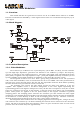
The video signal peak is detected through IC8 and through IC9 and it is differentiated with the
level adjusted through R45, in order to extract the dc component.
The IC9A output has a dc level related to the video signal not taking into account the
synchronizing pulses. The 100% video measurement is adjusted through R72 in the meter with a video
signal with 100% APL. The C118 e L18 components form an ICPM corrector circuit that allows
correcting a non-desirable phase-shift at the video carrier caused by the modulating signal.
The modulated video carrier is amplified by IC1 and the SAW filter FL1 filters this signal giving
the final characteristics of the desired modulation, i.e., AM_VSB (amplitude modulation with vestigial
side band). The amplifiers IC2, IC3 and IC4 produce the necessary gain to signal, in order to
compensate the losses in SAW filter and deliver a 0 dBm output level. The output signal level is
adjustable by R12 (front panel), which controls the PIN diode conduction (D1). The trimpot R13 limits
the maximum IF output level and the circuit formed by transistor Q19 and capacitor C120 increases
slowly the output level to eliminate high frequency peaks when the equipment is turned on.
The IF signal, after amplification, passes through a low-pass filter, formed by L6, L7, C21, C22
and C23 to eliminate harmonic signals. Part of this signal is sent to the detector circuit formed by
transistors Q3 and Q4 to measure the IF signal in the panel. The trimpot R24 allows adjusting the
reading level through the meter.
1.3.2. Audio Modulator:
The transistor Q14 and associated components generate the audio carrier. The applied voltage
to the varicap diode D10 controls its frequency. The amplifiers IC12 and IC13 increase the signal level
and through the trimpot R108 is applied to the IF amplifier to be delivered at the output. A sample of
this signal is delivered to the “prescaler” IC14 through R108. It divides the signal into 64 and delivers it
to PLL (integrated IC15). The PLL divides again this signal, now into 66, and compares it with a
reference signal in phase, resulting a voltage proportional to the difference of the phase between the
signals; this voltage is filtered and applied to diode D10 to correct the frequency. The reference
frequency for PLL is generated at the integrated circuit itself that oscillates at 10 MHz and divides it
into 1024. The oscillator crystal is found in a thermal chamber, which is controlled by Q15 and by
thermistor NT1, for better frequency stability. The trimmer C90 allows the fine adjustment of this
carrier frequency (41.25 MHz). If the circuit cannot correct the frequency, the transistors Q17 and Q18
are commuted to turn on the frequency error red led.
The audio signal that will cause the modulation in frequency in this carrier may come from the
mono audio input or stereo audio input. It is possible to select it through jump JP3.
The mono audio input circuit has an unbalanced amplifier IC10 and pre-emphasis circuit. It is
possible to turn off the pre-emphasis through jump JP2. The trimpot R92 (front panel) adjusts the
audio level that will cause the correct modulation index. The integrated circuit IC17 and associated
components form a peak detector of audio signal and a trimpot R117 allows adjusting 100% at the
meter for the correct deviation. The battery input (+36V) through D16 and fuse F1 connects through
connector CN2 the power supply FTE017 (optional).
Obs: The circuit diagram is divided into four parts.