Leddar Vu8 User Guide LeddarTech Inc. 2740 Einstein Street Quebec, Quebec G1P 4S4 CANADA www.leddartech.
Copyright © 2017 LeddarTech Inc. All rights reserved. The Company shall not be liable for any errors contained herein or for any damages arising out of or related to this document or the information contained therein, even if the Company has been advised of the possibility of such damages. The information contained herein is the property of LeddarTech Inc., and shall not be reproduced in whole or in part without prior written approval of LeddarTech Inc. LeddarTech Inc.
Table of Contents Introduction ..................................................................... 6 1.1. Description ....................................................................................... 6 1.2. SPI Carrier Board ............................................................................. 8 1.3. USB, CAN and SERIAL Carrier Board .................................................... 9 1.4. Working Diagram ............................................................................
5.4. Serial Link Interface ........................................................................ 48 5.5. CAN Bus Interface ........................................................................... 62 Leddar™ Configurator ..................................................... 72 6.1. Introduction to Configurator Software ................................................ 72 6.2. Connection Window ......................................................................... 73 6.3.
Help .............................................................................. 114 Index....................................................................................
Introduction The LeddarVu module enables developers and integrators to make the most of Leddar™ technology through integration in detection and ranging systems. The purpose of the LeddarVu module is to easily and rapidly be integrated in various applications. The module can be configured to be used in very simple applications or to perform more complex tasks depending on the hardware and software settings. 1.1.
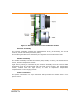
Figure 1: General elements of the LeddarVu module Receiver assembly The receiver assembly contains the photodetector array (8 elements), the circuit receiver, and an M7 Atmel processor (MCU). The module generates a full waveform per segment at its measurement rate. Emitter assembly The emitter assembly includes the emitter (LED, VSCEL, or laser), the emitter driver circuit, and the temperature sensor.
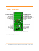
1.2. SPI Carrier Board The following presents the description of the SPI board. Figure 2: Board of the SPI LeddarVu module *Power outputs can supply up to 15 mA 8 P/N 54A0028-2 012017© 2017 LeddarTech Inc. Printed in Canada. All rights reserved.
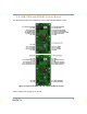
1.3. USB, CAN and SERIAL Carrier Board The following presents the description of the USB, CAN and SERIAL board.
DIP Switches The DIP switches are used for the configuration of the serial port number 1.
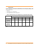
Table 2: Communication port configuration (for 8-position DIP switch) Interface DIP switch position 1 2 3 4 5 6 7 8 RS-232 OFF ON OFF OFF OFF X X X RS-485 two-wire configuration ON OFF ON ON ON X X X RS-422 ON ON OFF OFF OFF X X X RS-485 four-wire configuration NOTES: DIP switch position 6 on ‘ON’ position enables a 121Ω termination resistor to RS-485 two-wire configuration only (must be kept on ‘OFF’ position in any other configuration) DIP switch position 8 on ‘ON’
Table 3: Communication link configuration Pin position Interface RS-232 RS-485 two-wire configuration RS-422 1 GND GND GND 3 RTS D- Dout - 5 NC NC NC 7 RX D- Din + 9 TX D+ Dout + 11 CTS D- Din - RS-485 four-wire configuration NOTE: If a two-wire or four-wire differential port configuration is selected, in function of your network configuration, you should put bias resistors on transmitter or receiver lines to maintain the proper idle voltage and force the line to the idle condit
Table 4: S3 push button functionalities Description Action Long press during module operation (longer than 10 seconds) Resets the carrier board configuration to the default values: CAN port configuration 1Mbsp, standard frame format Base Rx: 0x740 Base Tx: 0x750 No delay Distance in cm and a max.
1.4. Working Diagram The working diagram explains how the module works in the standard and optional configurations. Figure 4: LeddarVu module working diagram 14 P/N 54A0028-2 012017© 2017 LeddarTech Inc. Printed in Canada. All rights reserved.
1.4.1. SPI Carrier Board The SPI carrier board includes the following elements: SPI and control interface The SPI serial port functionalities are available via pins 3, 5, 7, and 9. The port has a standard signal level of 0 V through 3.3 V. Table 5: SPI pin definition Pin 3 5 7 9 Function CLK (input) MISO (output) MOSI (input) CS (input) I2C interface The integrated circuit (I2C) protocol is intended to allow multiple slave digital circuits to communicate with one or more master circuit.
1.4.2. USB, CAN and SERIAL Board The optional carrier board includes the standard elements and the following ones: Serial ports (TTL, RS-232, RS-422, and RS-485) The TTL port is used for the short range transmission of data. The port has a standard signal level of 0 V through 3.3 V. The RS-232 is used for the transmission of data. It defines the signals connection between the data terminal equipment (such as a computer) and the data circuitterminating equipment (such as a modem).
Underlying Principles Created by LeddarTech, LEDDAR™ (light-emitting diode detection and ranging) is a unique sensing technology based on light (infrared spectrum) and the time-of-flight of light principle. The light source illuminates the area of interest (pulsed typically at 10 kHz for the Leddar Vu8 20° module) and the multichannel module receiver collects the backscatter of the emitted light and measures the time taken for the emitted light to return back to the module.
Getting Started This chapter presents the steps to install Leddar™ Configurator and start using the LeddarVu. 3.1. Optional power supply The power supply included with the Starter Kit version of the Leddar Vu8 has a pluggable terminal block that connects to the 12V header connector of the LeddarVu sensor. Location of the 12V header pin can be found on Figure 2 (LeddarVu SPI) or Figure 3 (LeddarVu USB, UART, CAN Bus).
3.2. Optional SPI cable The table below shows the pinout of the optional SPI cable sold by LeddarTech. Refer to Figure 2 for connection information. Table 6: Optional SPI Cable Pinout Wire Color Function Black Ground Blue Reset_N Orange SCLK Green MISO Yellow MOSI Brown CS# 3.3. Setup This section presents the Leddar™ Configurator installation and the procedure to set up the LeddarVu module. All software operations are described in chapter 6.
Figure 7: Welcome to the Leddar™ Software 3 Setup Wizard dialog box 3. In the End-User License Agreement dialog box, read the terms of the agreement, select the I accept the terms in the License Agreement check box, and click Next. Figure 8: End-User License Agreement dialog box 20 P/N 54A0028-2 012017© 2017 LeddarTech Inc. Printed in Canada. All rights reserved.
4. In the Product Types dialog box, the Leddar™ Development Kit check box is selected by default. Software Figure 9: Product Types dialog box 5. Click Next. 6. In the Destination Folder dialog box, click Next to select the default destination folder. OR Click the Change button to choose a destination folder. 7. In the Ready to Install Leddar™ Software 3 dialog box, click the Install button. 8. In the Completed the Leddar™ Software 3 Setup Wizard dialog box, click Finish.
3.4. Connecting to the LeddarVu Module The first time the module is connected to a computer, a few seconds are required for Windows™ to detect it and complete the installation. Once the installation is completed, you can connect to the LeddarVu module to create your configuration. To connect to the module: 1. Connect the power cable to the module and to a power source. 2. Connect the USB cable to the module and to the computer. 3. On the computer desktop, double-click the Leddar™ Configurator icon. 4.
5. In the Connection dialog box, in the Select a connection type list, select either LeddarVu SPI for a standard board or LeddarVu Serial for an USB, CAN and SERIAL. Figure 11: Connection dialog box 6. In the Available ports list, select the product and click the Connect button. The main window displays the detections (green lines) in the segments (white lines).
Figure 12: Main window A complete description of Leddar™ Configurator features and parameters for the LeddarVu module can be found at chapter 6. 24 P/N 54A0028-2 012017© 2017 LeddarTech Inc. Printed in Canada. All rights reserved.
Measurements and Settings This chapter presents measurements, settings, and zone definition for the LeddarVu module. 4.1. Distance Measurement Distance is measured from the base of the standoffs for the LeddarVu module. Figure 13: Distance measurement The dashed lines illustrate 1 of the 8 segments and the solid line indicates the distance measured by the module in that segment.
4.2. Data Description Data displayed in the Raw Detections dialog box allow the user to precisely define the desired detection parameters (View menu> Raw Detections). Figure 14: Raw Detections dialog box An object crossing the beam of the module is detected and measured. It is qualified by its distance, segment position, and amplitude. The quantity of light reflected back to the module by the object generates the amplitude. The bigger the reflection, the higher the amplitude will be.
The Flag parameter provides the status information that indicates the measurement type. Table 8: Flag value description Bit position Bit = 0 Bit = 1 0 Invalid measurement Valid measurement 1 Normal measurement Measurement is the result of demerge processing 2 Reserved Reserved 3 Normal measurement Received signal is above the saturation level. Measurements are valid (VALID is set) but have a lower accuracy and precision. Consider decreasing the light source intensity.
4.3. Acquisition Settings Acquisition settings allow you to define parameters to use for detection. To open the Acquisition Settings dialog box, on the Device menu, point to Configuration and click Acquisition. Figure 15: Acquisition Settings dialog box The numbers on a grey background are modified only by using the arrows, while the ones on a white background can additionally be modified manually by the numeric keypad of your keyboard. To apply new acquisition settings, click the apply button ( 28 ).
Table 10: Acquisition setting description Parameter Description Effect Accumulation Number of accumulations Higher values enhance the range, and reduce the measurement rate and noise. Oversampling Number of oversampling cycles Higher values enhance the accuracy/precision/resolution and reduce the measurement rate. Points Number of base sample points Determines the maximum detection range.
Accumulation When you increase the accumulation value, you reduce the noise as well as the measurement rate. Depending on your application, a reduction of the noise might be more important than a high measurement rate. Oversampling When you increase the accumulation value, you increase the resolution (accuracy) but you reduce the measurement rate. Depending on your application, a higher resolution might be more important than a high measurement rate. Points Determines the maximum detection range.
The multiple lines on each graph present the thresholds for numbers of accumulations of 1 (top curve), 2, 4, 8, 16, 32, 64, 128, and 256 (bottom curve). Accumulations of 512 and 1024 are also available, although not shown (provide the lowest thresholds). The threshold offset parameter has the effect of offsetting each value in the threshold table by the selected value. This provides a means of reducing the sensitivity (positive value) or increasing the sensitivity (negative value) of the module.
15.05 Estimated Measured True 15.04 Distance (m) 15.03 15.02 15.01 15 14.99 14.98 0 20 40 60 80 100 Sample Figure 17: Measurement smoothing example The red line represents the true target distance; the blue curve corresponds to the target distance measured by the module without smoothing, while the green curve is the smoothed measurements. One could notice the measurement precision (standard deviation) is dramatically improved by the smoothing algorithm.
Keeping the module in automatic light source power mode (default setting) ensures it adapts to varying environments. Close range objects may reflect so much light they can saturate the module, reducing the quality of the measurements. This mode will adapt the light output within the change delay setting to reach the optimal amplitude. On the other hand, low amplitudes provide lower accuracy and precision.
4.4. Measurement Rate The LeddarVu module acquires a base input waveform for each segment at a rate between 10 kHz and 40 kHz, depending on the sensor field of view (see Table 11). Multiple acquisitions are used to perform accumulations and oversampling, and generate a final waveform that is then processed to detect the presence of objects and measure their position.
Table 12: Measurement rate for Leddar Vu8 100° Accumulation Oversampling Measurement Rate (Hz) LeddarVu 20° LeddarVu 48° LeddarVu 100° 1024 8 0.15 0.3 0.61 512 8 0.3 0.6 1.22 256 8 0.6 1.2 2.4 128 8 1.22 2.4 4.8 64 8 2.4 4.8 9.7 32 8 4.8 9.7 19.5 1024 4 0.3 0.6 1.2 512 4 0.6 1.2 2.4 256 4 1.2 2.4 4.8 128 4 2.4 4.8 9.7 64 4 4.8 9.7 19.5 32 4 9.7 19.5 39.0 4.5.
The load (CPU Load) is displayed in the Device State window (View menu> State). It is recommended to verify the load when modifying the accumulations, oversampling, and point count parameters. The measurement rate will be lower than the calculated rate and the measurement period may be irregular when the load nears or reaches 100%. Figure 18: Device State window 36 P/N 54A0028-2 012017© 2017 LeddarTech Inc. Printed in Canada. All rights reserved.
Communication Interfaces The interfaces and links are optional and are implemented depending on your configuration. 5.1. SPI Interface The SPI interface on the SPI board is a direct link to the receiver module. The SPI interface available with the USB, CAN and SERIAL board is a port connected to MCU but not implemented for the moment. 5.1.1. SPI Basics The SPI interface uses the configuration mode 0; where, data is captured on the rising edge of the clock signal and outputted on the falling.
Table 13: Basic modes Mode Clock Polarity CPOL Clock Phase CPHA 0 0 0 1 0 1 2 1 0 3 1 1 5.1.2. SPI Protocol The universal SPI protocol uses a combination of standard commands for FLASH and SRAM memories. Each SPI packet contains a header, a payload, and a cyclic redundancy check (CRC). The first byte of the header corresponds to an instruction opcode. It is followed by a 24-bit address and the 16-bit size of the payload. The payload contains a number of user-data bytes.
Table 15: SPI opcode commands Mnemonic READ WRITE Opcode 0x0B 0x02 Operation Description Read data The read command returns data from memory starting at the selected address. It needs a delay between the group containing the opcode, address, and size data, and the return data stream to let the receiver module to decode the request and get the ready data to the clock. Write data The write command writes data to memory starting at the selected address and is limited to a page of 1 to 512 bytes.
The status register and bit flags are presented in Table 16. Table 16: Status register Bit Name Access Reserved R/W 1 Write enable latch R 0 Module ready R 7:2 Description Future use 0 = Write disabled 1 = Write enabled 0 = Module ready 1 = Module busy (programming, erasing) Data chronograms are represented in Figure 20 and Figure 21, and opcode and register chronograms are presented in Figure 22 and Figure 23.
5.1.3. Memory Map The memory map is divided in four memory banks. This section presents the description of the four memory banks in a table format.
through 16. 68 1 uint8_t Precision enabled 69 1 uint8_t Saturation compensation enabled 70 1 uint8_t Overshoot management enabled 71 4 int32_t Sensitivity (detection threshold) setting expressed in a raw amplitude scale. 75 1 uint8_t Light source power (0 to 100) 76 1 uint8_t Auto light source power enabled 77 2 uint16_t Auto frame average: Changes the delay in the number of measurements. This is the responsivity of the auto light source power according to the number of frames.
string 160 32 char Build date as an ASCII string 192 32 char Firmware version as an ASCII string 224 32 char Bootloader version as an ASCII string 256 32 char ASIC version as an ASCII string (optionally filled in function of the module) 288 32 char FPGA version as an ASCII string Module type 0x00000000: Invalid Device 0x00000007: M16 Evaluation Kit 320 2 uint16_t 0x00000008: IS16 0x00000009: M16 0x0000000A: Leddar One 0x0000000D: Leddar Vu8 322 4 uint32_t Internal Use 326 1 uin
349 4 uint32_t Clock frequency 353 1 uint8_t 354 4 uint32_t 358 1 uint8_t 359 4 uint32_t 363 2 int16_t Precision min. 365 2 int16_t Precision max. 367 4 int32_t Sensitivity min. 371 4 int32_t Sensitivity max. 375 1 uint8_t Current light source power count (max 16) 376 2 uint16_t Auto frame average min. 378 2 uint16_t Auto frame average max. 380 1 uint8_t Auto light source power percent min. 381 1 uint8_t Auto light source power percent max.
Detection list Table 20: Detection list bank Offset length Type Description 0 4 uint32_t Timestamp: in ms since the power up 4 2 uint16_t Number of detection (N) 6 2 uint16_t Current percentage of light source power 8 4 uint32_t Acquisition options 12 N* detection structure size Array of detection structure Start of detection list array Refer to Table 21 for details.
Transaction configuration Table 22: Transaction configuration bank Offset length Type Description Secure-transaction enabled flags: 0 1 uint8_t 1 = Enables the CRC calculation and validation on any transaction. This flag is enabled by default. 0 = No CRC validation. The CRC field is still required in SPI protocol but can be set to any value. Transaction modes: 0 = Free run. The READY pin is asserted on each ready detection frame. The host must be able to read data on time.
READY pin and manage the transaction mode. 5.1.4. SPI Operation The SPI operation includes four parameters: SPI port configuration, speed and timing, access, and modification. SPI port configuration The SPI port must be configured in the 0 mode (refer to section 5.1.1 on page 37) to communicate with the receiver module.
5. Send the write disabled command (write protection) to prevent any unwanted parameter change. NOTE: To prevent any data corruption or loss after modifying a parameter or a firmware update, the module must be in the ready state before shutting it down or doing a hard reset. 5.2. I2C Interface The I2C interface on the SPI board is a direct link to the receiver and source modules. For the moment, only the temperature sensor is accessible.
0 = Detections not ready 1 = Detections ready: this status flag is reset to 0 after reading this register 2 Number of segments (N) 11 Number of detections 12 Current percentage of light source power 13 Bit field of acquisition status: Reserved 14 Low 16 bits of timestamp (number of milliseconds since the module was started) 15 High 16 bits of timestamp 16 to 16 + N-1 Distance of first detection for each segment, zero if no detection in a segment.
16 + (9*N) to 16 + (10*N) - 1 Distance of the fourth detection 16 + (10*N) to 16 + (11*N) - 1 Amplitude of the fourth detection 16 + (11*N) to 16 + (12*N) - 1 Flag of the fourth detection 16 + (12*N) to 16 + (13*N) - 1 Distance of fifth detection 16 + (13*N) to 16 + (14*N) - 1 Amplitude of fifth detection 16 + (14*N) to 16 + (15*N) - 1 Flag of the fifth detection 16 + (15*N) to 16 + (16*N) - 1 Distance of the sixth detection 16 + (16*N) to 16 + (17*N) - 1 Amplitude of the sixth detection 16
fractional part (i.e. threshold value is this register divided by 64). 5 Light source power in percentage of the maximum. A value above 100 is an error. If a value is specified that is not one of the pre-defined values, the closest pre-defined value will be used. The register can be read back to know the actual value set.
value ranging from –16 through 16. 12 Low 16 bits of segment enabled: Bit-field of enabled segment 13 High 16 bits of segment enabled NOTE: As per the Modbus protocol, register values are returned in big-endian format. A request for a register that does not exist will return error code 2. Trying to set a register to an invalid value will return error code 3. If an error occurs while trying to execute the function, error code 4 will be returned.
The first byte is the number of detections in the message. Because of the limitation on a Modbus message length, a maximum of 40 detections will be returned. NOTE: This maximum can be configured to a lower value using the Leddar™ Configurator software (serial port configuration) or the Write Register command described below.
4 1 Number of bytes to read: 1 through 247 Table 29: Answers Offset Length Description 0 4 Base address: 0x00FFFFFF 4 1 Number of bytes read: 1 through 247 5 Nb * 1 byte 0x00000000 to Data Write module data (function code 0x43) Table 30 and Table 31 present the request and answer codes for writing data.
Read status = 0x05 Write enabled = 0x06 Write disabled = 0x04 Reset configuration = 0x C7 Soft reset = 0x99 1 1 Argument: optional value (must be set to 0x00) Table 33: Answers Offset Length Description 0 1 Opcode 1 1 Return value: optional return value (read status opcode = Status value) Get serial port settings (function code 0x45, 0x00) Table 34, Table 35 and Table 36 present the requests and answers of the get serial port settings.
Table 36: Answers serial port settings field Offset Length Description 0 1 Logical serial port number 1 4 Baud rate, supported rates: 5 1 9,600 19,200 38,400 57,600 115,200 Date size: 8 = 8-bit size 6 1 Parity: 0 = None 1 = Odd 2 = Even 7 1 8 1 Stop bit: 1 = 1 stop bit 2 = 2 stop bits Flow control: 0 = None 9 1 Modbus address: 1 through 247 10 1 Max. echoes per transactions. Used for the Get Detection command (function code 0x41), max. of 40 echoes.
Table 37: Requests header field Offset Length 0 1 Description Sub-function code: 0x01 Table 38: Requests serial port setting field Offset Length Description 0 1 Settings of corresponding logical serial port number to set. 1 4 Baud rate, supported rates: 5 1 9,600 19,200 38,400 57,600 115,200 Date size: 8 = 8-bit size 6 1 Parity: 0 = None 1 = Odd 2 = Even 7 1 8 1 Stop bit: 1 = 1 stop bit 2 = 2 stop bits Flow control: 0 = None 9 1 Modbus address: 1 through 247 10 1 Max.
Table 39: Answers Offset Length 0 1 Description Sub-function code: 0x01 Get carrier firmware information (function code 0x45, 0x02) Table 40 and Table 41 present the registers for the firmware information commands. Table 40: Requests Offset Length 0 1 Description Sub-function code: 0x02 Table 41: Answers Offset Length 0 1 1 32 33 8 Description Sub-function code: 0x02 Firmware part number ASCII string Firmware version in four units for format A, B, C, and D.
Table 43: Answers Offset Length Description 0 1 1 32 Hardware part number ASCII string 33 32 Hardware serial number ASCII string 65 4 Sub-function code: 0x03 Option bits. For Leddar use Get CAN port settings (function code 0x45, 0x04) Table 44, Table 45 and Table 46 present the requests and answers of the get CAN port settings.
Table 46: Answers CAN port settings field Offset Length Description 0 1 Logical CAN port number settings 1 4 Baud rate, supported rates: 10,000 20,000 50,000 100,000 125,000 250,000 500,000 1,000,000 5 1 6 4 Frame format: 0 = Standard 11 bits 1 = Extended 29 bits Tx base ID 10 4 Rx base ID 14 1 Maximum number of detections (measurements) returned per CAN detection message transaction: 1 through 96 15 2 Distance resolution: 17 2 19 2 1=m 10 = dm 100 = cm 1,
Set CAN port settings (function code 0x45, 0x05) Table 47 and Table 48 present the requests and answers for the CAN port commands.
Table 49: Answers Offset Length 0 1 Description Sub-function code: 0x05 5.5. CAN Bus Interface The CAN bus interface uses two default message IDs that can be modified by the user: 1856 (0x740) and 1872 (0x750).
Table 51: CAN bus request message Function Request (Byte 0) Function Request Description 1 Stop sending detections continuously 2 Send detection once Function Arguments (Byte 1) Bit field of operation mode Bit-0: 0 = Return detection in single message mode 1 = Return detection in multiple message mode 3 Start sending detections continuously (that is, the module will send a new set of detections each time they are ready without waiting for a request).
Table 52: CAN bus request message (Get input data) Input Data Type (Byte 1) Input Data Description 0 Number of segments 1 Device identification and option 2 and 3 Firmware version 4 and 5 Bootloader version 6 FPGA version 7 through 12 Serial number 13 through 18 Device name 19 through 24 Hardware part number 25 through 30 Software part number Table 53: CAN bus request message (Get holding data) Holding Data Type (Byte 1) 64 Holding Data Description 0 Acquisition configuration 1 Smo
Table 54: CAN bus request message (Set holding data) Holding Data Type (Byte 1) 0 1 2 3 Holding Data Description Acquisition configuration Smoothing and detection threshold Light source power management Distance resolution and acquisition options Argument Argument Description Byte 2 Exponent for the number of accumulation (that is, if the content of this register is n, 2n accumulations are performed).
Bytes 4 and 5 Bit field of acquisition options: Bit-0: Automatic light source power enabled Bit-1: Demerge object enabled Bit-2: Static noise removal enabled Bit-3: Precision enabled Bit-4: Saturation compensation enabled Bit-5: Overshoot management enabled 4 CAN port configuration 1 Byte 2 Baud rate (kbps): Byte 3 0 = 1000 1 = 500 2 = 250 3 = 125 4 = 100 5 = 50 6 = 20 7 = 10 Frame format: 0 = Standard 11 bits 1 = Extended 29 bits Bytes 4 through 7 Tx base ID 5 CAN port configurat
Table 55: CAN bus request message (Set base address) Data Description Argument Base address Bytes 4 through 7 Argument Description Base address to access (from 0x00000000 to 0x00FFFFFF) Table 56: CAN bus request message (Read module data) Data Description Argument Read module data Byte 1 Bytes 2 and 3 Argument Description Data length (1, 2, or 4) Offset from 0x0000 to 0xFFFF (final address to access is the result of the base address plus this offset).
1872 (0x750) (Tx base ID) These are 8-byte answer messages to the host command requests. Table 59: CAN bus answer message Answer Data (Byte 0) 1 2 3 4 5 6 7 8 9 10 68 Answer Data Description Additional Answer Data (Byte 1 to Byte 7) Answer to stop continuously sending detection requests. Success: Return echo from the command request. Answer to send once a detection request. Success: Return echo from the command request. Answer to continuously sending a detection request.
Table 60: CAN bus answer message (Get input data) Input Data Type (Byte 1) Input Data Description 0 Number of segments Bytes 2 and 3 Number of segments 1 Device identification and options Bytes 2 and 3 Device IS16) Bytes 4 through 7 Device option internal use) Bytes 2 and 3 The firmware build version (A) Bytes 4 and 5 The firmware build version (B) Bytes 6 and 7 The firmware build version (C) 2 Firmware version in format A, B, C, D.
Table 61: CAN bus answer message (Read module data) Data Description Argument Argument Description Read module opcode command Byte 1 Data length (1, 2, or 4) Byte 2 Offset Byte 3 Byte 4 Data to read Byte 5 Byte 6 Byte 7 Table 62: CAN bus answer message (Send module opcode request) Data Description Argument Argument Description Send module opcode command Byte 2 Opcode Byte 3 Optional argument Byte 4 Optional return value 1873 (0x751) (Tx base ID + 1) These are 8-byte messages that indica
1874 (0x752) (Tx base ID + 2) These are the detection messages with flag information, which contains one detection presented in the following format: Data bytes 0 and 1 contain the distance in units defined by the distance-units holding data. Data bytes 2 and 3 contain the amplitude. This value must be divided by 64 to get the amplitude (that is, 6 bits for fractional part). Data bytes 4 and 5 contain the flag information as described in the table below. Bytes 6 and 7 contain the segment number.
Leddar™ Configurator Leddar™ Configurator provides configuration functionalities for LeddarTech products. parameters and operation 6.1. Introduction to Configurator Software The Configurator interface can be resized manually or set to full screen view. All dialog boxes that do not include a selection of action buttons at the bottom, such as Connect, OK, Cancel, etc. are dockable at the top, the bottom, or on the right side of the main window.
6.2. Connection Window The following is a description of the information shown in the Connection dialog box. Figure 25: Connection dialog box Select a connection Type The connection type you are using. Available ports list The list of available ports displays the modules currently detected. NOTE: The next descriptions apply to IS16/M16/Evaluation Kit USB. Name The device name can be modified (see section “6.4.1 Module Name” on page 81).
6.3. Leddar™ Configurator Main Window After connecting to the device, the main window opens. Vertical scale setting areas Horizontal scale setting areas Figure 26: Leddar™ Configurator main window The measurements are plotted in a symbolic graph containing the 16 segments (white lines) originating from the LeddarVu module. Detections are drawn as arcs in their corresponding segments. Only valid measurements are displayed.
6.3.3. Force Equal Horizontal and Vertical Scales When the equal scaling button ( ) is selected (button highlighted), the original ratio of the display is kept or restored. The horizontal and vertical scales will be set to the same values and the beam will be displayed in accordance with the beam properties (for example, the display will show a 48° beam for a 48° LeddarVu module). Click the button again to change the vertical and horizontal scales independently.
To zoom the display horizontally, hold down the key of the computer keyboard while using the mouse wheel. NOTE: The equal scaling button ( ) must be not selected (not highlighted). Figure 27: Zooming in (left) and out (right) horizontally To zoom the display vertically, hold the key down while using the mouse wheel. NOTE: The equal scaling button ( 76 ) must be not selected (not highlighted). P/N 54A0028-2 012017© 2017 LeddarTech Inc. Printed in Canada. All rights reserved.
Figure 28: Zooming in (left) and out (right) vertically The measurements of a detection point appear as a pop-up when you point to it with the mouse cursor for a more accurate assessment of the detection. Detection points are shown in the form of green lines (arcs) in the main window for visibility reasons.
6.3.8. Changing the LeddarVu Module Origin The module origin can be modified by clicking the module origin at the bottom of the segments. To do so, use the mouse cursor to point to the bottom of the segments (a red dot appears); click and drag it in the desired position. Figure 30: Dot indicator to modify the module origin If you click and drag the module origin, its position is displayed in the status bar as shown in Figure 31. 78 P/N 54A0028-2 012017© 2017 LeddarTech Inc. Printed in Canada.
Figure 31: Module position changed To apply the changes, click the apply button ( ). The origin is saved in the module and it can also be modified by editing the parameters in the module position settings window. 6.3.9. Changing the LeddarVu Module Orientation The module origin may be rotated to match its physical position. If you do so, the main window display can better match the physical installation of the module.
Figure 32: Red bar to rotate the module position To apply the changes, click the apply button ( ). The module orientation is saved in the module and can also be modified by editing the parameters in the module position settings window. 6.4. Settings The LeddarVu module stores a number of settings. Once saved in the module, these parameters are effective at each power up. The Leddar™ Configurator software loads these parameters upon each connection. 80 P/N 54A0028-2 012017© 2017 LeddarTech Inc.
6.4.1. Module Name When you connect to a LeddarVu module for the first time, it has a default name. You can change that name at any time. To change the module name: 1. Connect to a module. 2. On the Device menu, point to Configuration and click Device Name. Figure 33: Device menu and the Configuration menu items 3. In the Device Name dialog box, in the Name field, type the new name of the module and click OK. Figure 34: Device Name dialog box 4.
6.4.2. Acquisition Settings The acquisition settings allow you to define parameters to use for detection and distance measurement. To open the Acquisition Settings dialog box, on the Device menu, point to Configuration and click Acquisition. Figure 35: Acquisition Settings dialog box The numbers on a grey background are modified only by using the arrows, while the ones on a white background can additionally be modified manually by using the numeric keypad of your keyboard.
6.4.3. Serial Port The serial port settings of the USB, CAN and SERIAL board are configurable. To configure the serial port: 1. On the Device menu, point to Configuration, Communication, and click Serial Ports. point to Figure 36: Device menu 2. In the Serial Port Setting dialog box, use the arrows or type numbers to modify the values.
Table 65 describes the serial port settings. Table 65: Serial port setting description Parameter Value Port number Select 1 for the configurable serial link number 1. Select 2 for the TTL serial link number 2. Select 3 for the USB VCP serial link. Baud rate 9600, 19200, 38400, 57600, 115200 bps Address 1 to 247 Detections 0 to 40 Distance resolution Millimeters (mm), centimeters (cm), decimeters (dm), meters (m) 6.4.4.
Figure 39: CAN Port Settings dialog box Table 68 describes the CAN port settings. Table 66: CAN port setting description Parameter Value Port number Select 1 for CAN communication Baud rate 10000, 20000, 50000, 100000, 125000, 250000, 500000, 1000000 bps Base Tx ID The base CAN arbitration ID used for data messages coming from the USB, CAN and SERIAL to host (see the protocol documentation).
6.5. Saving and Loading a Configuration The software configuration for a device can be saved to a file. This enables you to backup settings and restore them in case of system failure or in case you want to revert to earlier settings. You can also get the configuration that was stored with a record file. To save a configuration: On the File menu, click Save Configuration. Figure 40: File menu To load a configuration: On the File menu, click Load Configuration. 6.6.
2. In the Preferences dialog box, click Recording and click Recorder. Figure 42: Preferences dialog box 3. Under Directory, click the Browse button to select the path where you want to save the detection record file. 4. In the Maximum file size box, set the maximum file size by using the arrows or by entering the value manually. 5. Under What, select one of the Debug check boxes. 6.
Figure 43: File menu To stop a recording manually: On the File menu, click Stop Recording. Figure 44: File menu to stop a recording The following is a description of the elements available in the Preferences for recording dialog box. Record directory The record directory is the folder in which all record files will be saved. These files are in a proprietary format, with the extension *.ltl, and can only be opened and viewed with the Leddar™ Configurator software.
Maximum record time The value entered as the Maximum record time determines the length of the time for recording. At the end of that period, recording will stop even if the file size has not reached its maximum. 6.7. Using Detection Records Once you have completed a recording, you can review it and extract part of the recording. The Record Replay dialog box offers the same functions as a regular video player: there is a stop button, a play button, and frame-by-frame forward and backward buttons.
Play button Figure 46: Record Replay dialog box 4. Click the play button to start the playback. To extract a record file segment: 1. Set the Position slider to the position where you want the file segment to start and click the Start button. 2. Set the Position slider to the position where you want the file segment to stop and click the End button.
Table 67: Field description of the log text file Time (msec) Segment [0 15] Amplitude [0 512] Distance (m) Status 12735204 7 0.9 33.61 1 The time of the detection is 12735204 milliseconds from the time the LeddarVu module was started. The location of the detection is segment 7 (the 8th segment). The amplitude of the detection is 0.09, which is very low (small, far, or dark object). The distance of the detection is 33.61 meters. The status indicates a normal measurement.
3. Under Directory, click the browse button to select the path where you want to save the log and click OK. 4. On the File menu, click Start Data Logging. Figure 49: File menu 5. To stop recording, on the File menu, click Stop Data Logging. Figure 50: File menu to stop data recording A .txt file is saved in the selected directory. 92 P/N 54A0028-2 012017© 2017 LeddarTech Inc. Printed in Canada. All rights reserved.
6.9. Device State Information about a device is accessible when connecting to a device in the Connection window or by clicking the State command on the View menu. Figure 51: View menu The Device State window opens.
General Timers & Load This feature gives information in days, hours, minutes, and seconds about two types of activities of a device. The first line indicates the time elapsed since the last device reset, the second since the last power cut or outage. Measurement Rate This parameter indicates the rate at which the module measures the speed and dimension of static or moving surfaces. Automatic Parameter Values This parameter indicates the intensity of the light source.
Software Part Number This parameter indicates the software part number of the device as assigned by LeddarTech. Manufacturer Name This parameter indicates the name assigned to LeddarTech. Group Id Number This parameter indicates the end-user group unique identifier used for licencing purposes Carrier Serial Number This parameter indicates the serial number of the USB, CAN and SERIAL carrier board as assigned by LeddarTech.
Figure 53: Settings Menu and Preferences Dialog Box Windows The two options allow the user to select how the content of the main window will be displayed in Leddar™ Configurator. Choices are: The Restore window position and size on startup feature starts Leddar™ Configurator at the same place on the computer desktop and at the same size it was when it was closed.
6.11. Raw Detections The Raw Detections dialog box allows you to view detection values in many ways. It provides filters to isolate segments and detection parameters.. To open the Raw Detections dialog box, on the View menu, click Raw Detections. Figure 54: View menu and Raw Detections dialog box Figure 55 presents an example of raw detections. When there is no detection in some segments, only the segments where a detection occurred appear in the list.
Figure 55: Example of detection filters The following is a description of the parameters available in the Raw Detections dialog box. Min and Max Amplitude The value entered in the Min Amplitude box shows only detections of amplitude higher or equal to that value. For example, if the minimum amplitude is set to 5, only the detections of amplitude 5 and more will be displayed. The value entered in the Max Amplitude box will show only detections of amplitude lower or equal to that value.
The value entered in the Max Amplitude box will show only detections at a distance smaller or equal to that value. For example, if the minimum distance is set to 20, only the detections at a distance of 20 and less will be displayed. Setting a value in both fields will result in a range of distance to display. Boxes 1 to 8 Check boxes 1 to 8 allow you to select which segments to display. Freeze When selected, the Freeze parameter freezes the values displayed in the Raw Detections dialog box.
Flag The Flag column displays a number that represents a detection type. Table 68: Flag value description Bit position 0 Bit 0 Invalid measurement Bit 1 1 Reserved Reserved 2 Reserved Reserved 3 Normal measurement 4 Reserved Received signal is above the saturation level. Measurements are valid (VALID is set) but have a lower accuracy and precision. Consider decreasing the light source intensity.
Specifications This chapter presents the LeddarVu module. 7.1. General Table 70: General specifications Light Source pulse rate 51.2 kHz Photodetector array size 1x8 Photodetector acquisition rate 100 MHz Measurement rate See Table 12 on page 35. USB (optional) 2.0, 12 Mbits/s CAN (optional) 10 to 1000 kbit/s, optional 120- termination Serial links (optional) TTL, RS-232, RS-422, and RS-485. 2-wire, 4-wire, 9600 to 115200 BPS Operating temperature -40°C to +85°C 7.2.
7.3. Electrical Table 72: Electrical specifications Voltage 12 VDC Power consumption (total) 2.2 W Power output maximum current 15 mA 7.4. Optical Table 73: Optical specifications Wavelength 905 nm (infrared) Laser risk group IEC 60825-1:2014 (Third Edition); Class I laser product (certification pending) Beam width and height See Table 74. Table 74: Beam width and height Beam Option Beam Width* Beam Height* 20° x 0.3° 16.4° 0.173° 20° x 3° 16.3° 3.12° 48° x 0.3° 56.3° 0.
Figure 56: Beam pattern width (left) and height (right) 7.5.
Figure 57: 20° x 0.3° (maximum intensity, 256 accumulations, and 8 oversamplings) 104 P/N 54A0028-2 012017© 2017 LeddarTech Inc. Printed in Canada. All rights reserved.
Figure 58: 20° x 3° (maximum intensity, 256 accumulations, and 8 oversamplings) 105
Figure 59: 48° x 0.3° (maximum intensity, 256 accumulations, and 8 oversamplings) 106 P/N 54A0028-2 012017© 2017 LeddarTech Inc. Printed in Canada. All rights reserved.
Figure 60: 48° x 3° (maximum intensity, 256 accumulations, and 8 oversamplings) 107
Figure 61: 100° x 0.3° (maximum intensity, 256 accumulations, and 8 oversamplings) 108 P/N 54A0028-2 012017© 2017 LeddarTech Inc. Printed in Canada. All rights reserved.
Figure 62: 100° x 3° (maximum intensity, 256 accumulations, and 8 oversamplings) 109
7.6. Regulatory Compliancy The module complies with FDA performance standards for laser products except for deviations pursuant to Laser Notice No. 50, dated June 24, 2007. NOTE: Testing results are valid for a cable length shorter than 3 meters.
7.7.1.
7.7.2. 48° Module Figure 64: 48° module dimensions 112 P/N 54A0028-2 012017© 2017 LeddarTech Inc. Printed in Canada. All rights reserved.
7.7.3.
Help For technical inquiries, please contact LeddarTech technical support by registering online at www.leddartech.com/support to easily: Follow up on your requests Find quick answers to questions Get valuable updates Or by contacting us at: + 1 418 653 9000 + 1 855 865 9900 8:30 a.m. - 5:00 p.m. Eastern Standard Time To facilitate the support, please have in hand all relevant information such as part numbers, serial numbers, etc. E-mail support@leddartech.com Company address LeddarTech Inc.
Index A Accumulation ................................ 29, 30 Accuracy .......................................... 103 Amplitude, raw detection ...................... 98 Asic version ........................................ 94 Atmel processor ................................... 7 Automatic parameter values ................. 94 C CAN bus ..................................... 16, 101 CAN port settings, Get ......................... 59 CAN port settings, Set..........................
USB ................................................ 16 L Laser .................................................. 7 LED .................................................... 7 Light Source Control............................................ 29 Intensity ................................... 29, 32 Pulse rate ...................................... 101 M Main window ....................................... 23 Manufacturer’s name ........................... 95 MCU processor .....................................
Light Source Intensity ....................... 29 Oversampling .................................. 29 Points ............................................. 29 Smoothing....................................... 29 Threshold offset ............................... 29 Smoothing .................................... 29, 31 Software Part number .................................... 95 Part number, USB, CAN and SERIAL carrier board ................................ 95 Source assembly ..................................