
User Manual
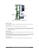


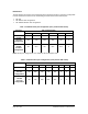
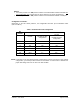


Table Of Contents
- List of Figures
- List of Tables
- 1. Introduction
- 1.1. Description
- 1.2. SPI Carrier Board
- 1.3. USB, CAN and SERIAL Carrier Board
- 1.4. Working Diagram
- 1.4.1. SPI Carrier Board
- 1.4.2. USB, CAN and SERIAL Board
- 2. Underlying Principles
- 3. Getting Started
- 3.1. Optional Power Supply
- 3.2. Optional SPI cable
- 3.3. Setup
- 3.4. Connecting to the LeddarVu Module
- 4. Measurements and Settings
- 4.1. Distance Measurement
- 4.2. Data Description
- 4.3. Acquisition Settings
- 4.3.1. General Settings
- 4.3.2. Enabling and Disabling Segments
- 4.4. Measurement Rate
- 4.5. CPU Load
- 5. Communication Interfaces
- 5.1. SPI Interface
- 5.1.1. SPI Basics
- 5.1.2. SPI Protocol
- 5.1.3. Memory Map
- Configuration Data
- Product Configuration
- Device Information and Constants
- LeddarVu Device Information and Constants
- General Status
- LeddarVu Status
- Detection List
- Transaction Configuration
- 5.1.4. SPI Operation
- 5.1.4.1. SPI Port Configuration
- 5.1.4.2. Sensor Hard Reset
- 5.1.4.3. Speed and timing
- 5.1.4.4. Access
- 5.1.4.5. Modification
- 5.2. I2C Interface
- 5.3. USB Interface
- 5.4. Serial Link Interface
- 5.5. CAN Bus Interface
- 6. Leddar™ Configurator
- 6.1. Introduction to Configurator Software
- 6.2. Connection Window
- 6.3. Leddar™ Configurator Main Window
- 6.3.1. Toolbar
- 6.3.2. Fit to Window
- 6.3.3. Force Equal Horizontal and Vertical Scales
- 6.3.4. Zoom in
- 6.3.5. Zoom out
- 6.3.6. Scale
- 6.3.7. Panning and Zooming
- 6.3.8. Changing the LeddarVu Module Origin
- 6.3.9. Changing the LeddarVu Module Orientation
- 6.4. Settings
- 6.4.1. Module Name
- 6.4.2. Acquisition Settings
- 6.4.3. Serial Port
- 6.4.4. CAN Port
- 6.5. Saving and Loading a Configuration
- 6.6. Configuring Detection Records
- 6.7. Using Detection Records
- 6.8. Data Logging
- 6.9. Firmware Update
- 6.10. Device State
- General
- Device Information
- Carrier
- 6.11. Preferences
- 6.12. Raw Detections
- 7. Specifications
- 7.1. General
- 7.2. Mechanical
- 7.3. Electrical
- 7.4. Optical
- 7.5. Performance
- 7.6. Regulatory Compliance and Safety
- 7.7. Dimensions
- 7.7.1. 98.5 Module
- 7.7.2. 47.5 Module
- 7.7.3. 16 Module
- 8. Technical Support
- Appendix A ̶ Example of a 0x04 function (read input register)
- Appendix B ̶ Example of a 0x41 Modbus Function
- Appendix C ̶ Example of a LeddarVu CAN Bus Detection Request

Page 19 of 129 54A0028-6 042019 © LeddarTech Inc.
1.4.1. SPI Carrier Board
The SPI carrier board includes the following elements:
SPI and control interface
The SPI serial port functionalities are available via pins 3, 5, 7, and 9. The port has a standard
signal level of 0 V through 3.3 V.
Table 5: SPI pin definition
Pin
Function
3
CLK (input)
4
Hard-reset (input)
5
MISO (output)
7
MOSI (input)
9
CS (input)
I2C interface
The integrated circuit (I2C) protocol is intended to allow multiple slave digital circuits to
communicate with one or more master circuit. As for the SPI, it is only intended for short distance
communications. The port has a standard signal level of 0 V through 3.3 V.
Power supply
The power source includes the source, the auxiliary DC output connection, the +12 V connection,
the +5 V analog supply, and the +3.3 V supply.