
Datasheet

Lighting Design Manufacturing Service
www.edison-opto.com.tw
Copyright © 2011 Edison Opto Corporation. All right reserved. The information in this document is subject to change without notice.
version : 8 21
Product Soldering Instructions
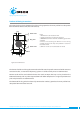
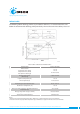
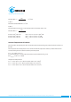
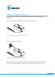
Figure 30. Pad dimensions
The central circle pad at the bottom face of the package provides the main path for heat dissipation
from the LED to the heat sink (heat sink contact).
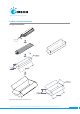
The choice of solder and the application method will dictate the specic amount of solder. For most
consistent results, an automated dispensing system or a solder stencil printer is recommended.
Positive results will be used solder thickness that results in 50μm. The lamp can be placed on the
PCB simultaneously with any other required SMD and reow completed in a single step. Automated
pick-and-place tools are recommended.
The bottom of the slug, which is electrically connected to anode(+), provides the main path for heat
dissipation from LED to the heat-sink.
6.00
Ø5.0
3.6
1.60
1.90
Slug Pad
Solder Pad
Solder Pad
Notes:
1. All dimensions are measured in mm.
2. Solder pad cannot be connected to slug pad.
3. MCPCB material with a thermal conductivity greater than
3.0 W/mK.
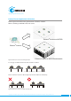
4. Please avoid touching the Edixeon® A lens during
assembly processes .This may cause pollution or scratch on
the surface of lens.
5. Edixeon® A series can not be heated over 150ºC.