Internal Use Only Website:http://biz.LGservice.com COLOR MONITOR SERVICE MANUAL CHASSIS NO. : LM57B MODEL: L1733TR (L1733TR-SFQ.A**MQP) L1933TR (L1933TR-SFQ.A**MQP,A**RQP) ( ) **Same model for Service CAUTION BEFORE SERVICING THE UNIT, READ THE SAFETY PRECAUTIONS IN THIS MANUAL. *To apply the MSTAR Chip.
CONTENTS SPECIFICATIONS ................................................... 2 PRECAUTIONS ....................................................... 3 TIMING CHART ....................................................... 7 DISASSEMBLY ....................................................... 8 BLOCK DIAGRAM...................................................12 DISCRIPTION OF BLOCK DIAGRAM .................. 14 ADJUSTMENT ...................................................... 16 SERVICE OSD .......................
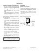
PRECAUTION WARNING FOR THE SAFETY-RELATED COMPONENT. WARNING • There are some special components used in LCD monitor that are important for safety. These parts are marked on the schematic diagram and the replacement parts list. It is essential that these critical parts should be replaced with the manufacturer’s specified parts to prevent electric shock, fire or other hazard.
SERVICING PRECAUTIONS CAUTION: Before servicing receivers covered by this service manual and its supplements and addenda, read and follow the SAFETY PRECAUTIONS on page 3 of this publication. NOTE: If unforeseen circumstances create conflict between the following servicing precautions and any of the safety precautions on page 3 of this publication, always follow the safety precautions. Remember: Safety First. General Servicing Precautions 1.
General Soldering Guidelines 1. Use a grounded-tip, low-wattage soldering iron and appropriate tip size and shape that will maintain tip temperature within the range or 500 F to 600 F. 2. Use an appropriate gauge of RMA resin-core solder composed of 60 parts tin/40 parts lead. 3. Keep the soldering iron tip clean and well tinned. 4. Thoroughly clean the surfaces to be soldered. Use a mall wire-bristle (0.5 inch, or 1.25cm) brush with a metal handle. Do not use freon-propelled spray-on cleaners. 5.
Circuit Board Foil Repair Excessive heat applied to the copper foil of any printed circuit board will weaken the adhesive that bonds the foil to the circuit board causing the foil to separate from or "lift-off" the board. The following guidelines and procedures should be followed whenever this condition is encountered. At IC Connections To repair a defective copper pattern at IC connections use the following procedure to install a jumper wire on the copper pattern side of the circuit board.
TIMING CHART VIDEO A E D B SYNC C Sync Video Duration Active (D) Time ( A ) 640 16 MODE H/V Sync Polarity Dot Clock Frequency 1 H(Pixels) + 25.175 31.469 Total Period (E) 800 V(Lines) - 70.09 449 350 2 H(Pixels) - 28.321 31.468 900 720 V(Lines) + 70.
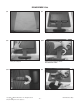
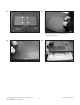
DISASSEMBLY-Set #1 #2 Soft pad on the table. #3 Monitor on the pad. # 4-1 Hold the head & stand base and then Pull up the stand part. Twist Stand until "Click". # 4-2 #5 Separate head & stand Copyright 2007 LG Electronics. Inc. All right reserved.
#6 #7 1. Pull the front cover upward. 2. Then, let the all latches are separated.(#3-1~3-2) 3. Put the front face down. Remove the screws. #8 #9 Disassemble back cover. Copyright 2007 LG Electronics. Inc. All right reserved.
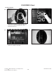
DISASSEMBLY-Stand * In case of Latch 4. # 1-1 # 1-2 Push the four latches on the bottom to the outside and Separate Stand Body & Base. (Reference the #1-2) #2 #3 After finished repair, necessarily push 4ea Latches to inside for restoration. Copyright 2007 LG Electronics. Inc. All right reserved.
DISASSEMBLY-Stand * In case of Latch 2. #1 #2 Hold the stand body. #3 Confirm two latch of right and left. #4 Push the latch to the inside. Push the base to the opposite direction. #5 Confirm the condition of separation. Copyright 2007 LG Electronics. Inc. All right reserved.
Copyright 2007 LG Electronics. Inc. All right reserved. Only for training and service purposes D-Sub DVI-D Filter EEPROM (EDID) Digital - 12 - Inverter (4 lamps) 12V LIPS Analog (R/G/B) 12V 5V 1.8V 3.3V 5V MCU Intel8032 TMDS Rx ADC TSUMx6AL 12V Regulator 1.8V 3.3V 3.3V Flash ROM Scaler Line Buffer 3.
Main Board (Scaler & DC DC converter) Module Vcc Copyright 2007 LG Electronics. Inc. All right reserved. Only for training and service purposes - 13 L N Line Filter Start Power Control IC Drive Aux Dimming (Lamp Current Control) Inverter On/OFF (3.
DESCRIPTION OF BLOCK DIAGRAM 1. Video Controller Part. This part amplifies the level of video signal for the digital conversion and converts from the analog video signal to the digital video signal using a pixel clock. The pixel clock for each mode is generated by the PLL. The range of the pixel clock is from 25MHz to 135MHz. This part consists of the Scaler, ADC convertor, TMDS receiver and LVDS transmitter.
LIPS Board Block Diagram 12V 50 ~ 60Hz LINE 100 ~ 240V EMI COMPONENTS INPUT RECTIFIER AND FILTER HVDC SWITCHING TRANSFORMER 100KHz OUTPUT RECTIFIER AND FILTER 5V GND PWM CONTROL CIRCUIT PHOTO-COUPLER ISOLATION PRIMARY 12V SIGNAL COLLENTION SECONDARY INVERTER CIRCUIT High Voltage Operation description_LIPS 1. EMI components.
ADJUSTMENT Windows EDID V1.0 User Manual 2. EDID Read & Write 1) Run WinEDID.exe Operating System: MS Windows 98, 2000, XP Port Setup: Windows 98 => Don’t need setup Windows 2000, XP => Need to Port Setup. This program is available to LCD Monitor only. 1. Port Setup a) Copy “UserPort.sys” file to “c:\WINNT\system32\drivers” folder b) Run Userport.
SERVICE OSD 1) Turn off the power switch at the front side of the display. 2) Wait for about 5 seconds and press MENU, POWER switch with 1 second interval. 3) The SVC OSD menu contains additional menus that the User OSD menu as described below. a) Auto Color : W/B balance and Automatically sets the gain and offset value. b) NVRAM INIT : EEPROM initialize.(24C08) c) CLEAR ETI : To initialize using time. d) AGING : Select Aging mode(on/off). e) R/G/B-9300K : Allows you to set the R/G/B-9300K value manually.
TROUBLESHOOTING GUIDE 1. NO POWER NO POWER (POWER INDICATOR OFF) Check J403 Voltage Pin5, Pin6 (5V)? NO Check Power Board, And Find Out a Short Point as Opening Each Power Line YES Check U301 Pin2 Voltage (3.3V) ? NO Check 3.3V Line (Open Check) No Problem YES Check Key Control Connector Routine Is U201 Pin75 (3.3V) Voltage ? NO Check 3.3V Line YES 1 Check U201 Pin 96 Pulse NO Check X-TAL YES Check U201 Waveforms 1 U201-#96 Copyright 2007 LG Electronics. Inc. All right reserved.
2. NO RASTER (OSD IS NOT DISPLAYED) – LIPS NO RASTER (OSD IS NOT DISPLAYED) J403 PIN5, PIN6 5V? NO CHECK POWER BOARD, AND FIND OUT A SHORT POINT AS OPENING EACH POWER LINE YES J403 PIN9 5V? NO CHECK MICOM INV ON/OFF PORT. YES J403 PIN10 5V? NO 1. CONFIRM BRIGHTNESS OSD CONTRL STATE. 2. CHECK MICOM DIM-ADJ PORT YES CHECK PULSE AS CONTACTING SCOPE PROBE TO CAUTION LABEL. (CONTACT PROBE TO CAUTION LABEL.
3. NO RASTER (OSD IS NOT DISPLAYED) – MSTAR NO RASTER (OSD IS NOT DISPLAYED) U201 PIN 16, 75 3.3V? NO CHECK U301 YES U201 PIN96, 97 OSCILLATE AS 14.31MHZ? 1 1. CHECK C210, C211 SOLDERING CONDITION 2. CHECK X201 3. TROUBLE IN U201 NO YES 2 U201 PIN27 IS 48KHz H-SYNC? PIN28 IS 60Hz V-SYNC? IS PULSE APPEARED AT SIGNAL PINS? AT MODE 12? CHECK CONNECTION LINE FROM D-SUB TO U201 NO YES TROUBLE IN CABLE OR LCD MODULE Waveforms 1 U201-#96, 97 2 2 U201-#27 H-SYNC Copyright 2007 LG Electronics.
4. TROUBLE IN DPM TROUBLE IN DPM NO CHECK R442, R443 3 CHECK PC PC IS NOT GOING INTO DPM OFF MODE YES CHECK U201 PIN 27,28 SYNC PULSE ? NO CHECK H/V SYNC LINE YES TROUBLE IN U201 Waveforms 3 R442 H-Sync 3 R443 V-Sync Copyright 2007 LG Electronics. Inc. All right reserved.
5. POWER NO POWER (POWER INDICATOR OFF) CHECK Fuse F101 OK? NO Trouble in Fuse (F101) YES CHECK C101 Voltage (AC110V->160Vdc (AC220V->304Vdc NO Check BD101 YES CHECK U101 Pin6 Waveform (Square wave Come out?) NO Check U101 Pin7 : 9~10V Check D102 YES Check Q101 Drain Waveform NO Trouble in Q101 YES Check D201, D202 Voltage NO Trouble in D201, D202 YES CHECK 5V, 12V Line Copyright 2007 LG Electronics. Inc. All right reserved.
6. Raster NO Raster (Lamp Off) CHECK P201 Pin9 3.3V? NO Check Scaler Output (Main Board) YES Check U301 Pin3 5V? NO Check Q301, Q302 YES Check U301 Pin2 OVP, Less than 1.8V NO Check the waveform of U301 Pin11, 12, 19, 20 NO Check the waveform of U301 Pin11, 12, 19, 20 YES Check U301 Pin10 CMP, Less than 2.75V If waveform is no problem Check U303, U304 Drain waveform NO Check Q303~Q308 Or Trouble in U303, U304 YES CHECK T301, T302 Copyright 2007 LG Electronics. Inc. All right reserved.
WIRING DIAGRAM 30P 6631900109A 11P 6631T20023J 6P 6631900011H 3P 6631T20010E-L1733TR 6631900125A-L1933TR Copyright 2007 LG Electronics. Inc. All right reserved.
120 060 010 070 080 020 090 050 100 040 110 190 130 140 170 180 030 150 160 EXPLODED VIEW Copyright 2007 LG Electronics. Inc. All right reserved.
EXPLODED VIEW PARTS LIST * Note: Safety mark Ref. No. 010 020 Part No. Description ABJ32220472 Cabinet Assembly, L1753 . 17" SILVER best buy for L1733TR ABJ32229471 Cabinet Assembly, L1953 . 19" SILVER L1933TR FOR BEST BUY EAJ32188801 LCD,Module-TFT, LM170E03-TLB3 DRIVER 17.0INCH 1280X1024 300CD COLOR 72% 5/4 800 VS 1 5MS, 160/160, 4LAMP, 2CH-LVDS LG PHILIPS LCD . EAJ32189001 LCD,Module-TFT, LM190E08-TLB2 DRIVER 19.
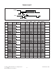
REPLACEMENT PARTS LIST CAUTION: BEFORE REPLACING ANY OF THESE COMPONENTS, READ CAREFULLY THE SAFETY PRECAUTIONS IN THIS MANUAL. MAIN BOARD AND POWER BOARD PARTS ARE DIFFERENT. * NOTE : S SAFETY Mark AL ALTERNATIVE PARTS *S *AL LOC. NO. PART NO. DATE: 2007. 02. 06. DESCRIPTION / SPECIFICATION *S *AL LOC. NO.
PART NO. DATE: 2007. 02. 06. DESCRIPTION / SPECIFICATION 0ISG240860B 0IMMR00203A 0IMMR00014A 0IMMR00014A 0IPMGFA003G 0IPMGSG016A 0IPMG78403A M24C08-WMN6TP 8KBIT 1KX8BIT-L1733TR FM24C08 8KBIT 1KX8BIT 2.7VTO-L1933TR M24C02-RMN6TP 2KBIT 256X8BIT M24C02-RMN6TP 2KBIT 256X8BIT FAN1117AS33X 4.8TO10.3V 3.3V LD1086D2T18TR 3.4TO30V 1.8V-L1733TR AZ1086S-1.8TRE1 3.2TO10V 1.
*S *AL LOC. NO. PART NO. DATE: 2007. 02. 06. DESCRIPTION / SPECIFICATION *S *AL LOC. NO.
*S *AL LOC. NO. R316 R317 R318 R319 R320 R321 R401 R402 R403 R404 R406 R407 R408 R409 TH101 PART NO. 0RH2001D622 0RJ3303E472 0RJ1503E472 0RH1303D622 0RH1502D422 0RH1002D422 0RJ1001G476 0RJ1001G476 0RJ1001G476 0RJ1001G476 0RJ3600E472 0RJ3600E472 0RJ3600E472 0RJ3600E472 6322A00035A DATE: 2007. 02. 06. DESCRIPTION / SPECIFICATION 2K OHM 1 / 10 W 2012 5.00% D 330000 OHM 1/8 W 1% 2012 R/T 150K OHM 1/8 W 1% 2012 R/TP 130K OHM 1 / 10 W 2012 5.
SCHEMATIC DIAGRAM 1. SCALER Copyright 2007 LG Electronics. Inc. All right reserved.
2. POWER & WAFER Copyright 2007 LG Electronics. Inc. All right reserved.
3. INVERTER Copyright 2007 LG Electronics. Inc. All right reserved.
4. POWER Copyright 2007 LG Electronics. Inc. All right reserved.
P/NO : MFL43002807 Feb.