Website:http://biz.LGservice.com E-mail:http://www.LGEservice.com/techsup.html COLOR MONITOR SERVICE MANUAL CHASSIS NO. : CA-136 MODEL: ( T730BH(K) (T730BHKL-K***E*) T730SH(K) (T730SHKL-K***E*) ) **Same model for Service CAUTION BEFORE SERVICING THE UNIT, READ THE SAFETY PRECAUTIONS IN THIS MANUAL. *Same looking with new chassis.
CONTENTS SPECIFICATIONS ................................................... 2 SAFETY PRECAUTIONS ........................................ 3 SERVICE PRECAUTION.......................................... 4 TIMING CHART ....................................................... 7 WIRING DIAGRAM ................................................. 9 DISASSEMBLY ....................................................... 8 BLOCK DIAGRAM ................................................... 10 DESCRIPTION OF BLOCK DIAGRAM...
SAFETY PRECAUTIONS SAFETY-RELATED COMPONENT WARNING! There are special components used in this color monitor which are important for safety. These parts are marked on the schematic diagram and the replacement parts list. It is essential that these critical parts should be replaced with the manufacturer's specified parts to prevent X-radiation, shock, fire, or other hazards.
SERVICING PRECAUTIONS CAUTION: Before servicing receivers covered by this service manual and its supplements and addenda, read and follow the SAFETY PRECAUTIONS on page 3 of this publication. NOTE: If unforeseen circumstances create conflict between the following servicing precautions and any of the safety precautions on page 3 of this publication, always follow the safety precautions. Remember: Safety First. General Servicing Precautions 1.
General Soldering Guidelines 1. Use a grounded-tip, low-wattage soldering iron and appropriate tip size and shape that will maintain tip temperature within the range or 500 F to 600 F. 2. Use an appropriate gauge of RMA resin-core solder composed of 60 parts tin/40 parts lead. 3. Keep the soldering iron tip clean and well tinned. 4. Thoroughly clean the surfaces to be soldered. Use a mall wire-bristle (0.5 inch, or 1.25cm) brush with a metal handle. Do not use freon-propelled spray-on cleaners. 5.
Circuit Board Foil Repair Excessive heat applied to the copper foil of any printed circuit board will weaken the adhesive that bonds the foil to the circuit board causing the foil to separate from or "lift-off" the board. The following guidelines and procedures should be followed whenever this condition is encountered. At IC Connections To repair a defective copper pattern at IC connections use the following procedure to install a jumper wire on the copper pattern side of the circuit board.
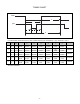
TIMING CHART Video B C Sync D E F A << Dot Clock (MHz), Horizontal Frequency (kHz), Vertical Frequency (Hz), Horizontal etc... (µs), Vertical etc... (ms) >> Mode 1 2 3 4 5 H/V Sort Sync Polarity Frequency H - 37.50 26.67 20.32 74.99 13.335 12.802 V Active Time (A) Video Time (B) Front Porch (D) Sync Time (E) 6.35 0.51 2.03 3.81 0.533 0.026 0.08 0.427 Blanking Time (C) Back Porch (F) H + 46.88 21.33 16.16 5.17 0.32 + 75.01 13.331 12.798 0.533 0.021 1.62 0.
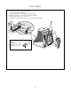
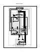
DIS A S S E MB LY 1. T IL T /S WIV E L & B A C K C OV E R R E MOV A L 1) S et the monitor face downward. 2) C arefully remove the T ilt/S wivel by pulling it upward. 3) Remove the screw (b), B ack cover by pus hing it upward. 4) R eleas e the latch (c). (S ee T ip S pec.) 5) S lide the B ack C over away from the F ront C abinet of the monitor. (b) B ac k Co v er (c) Ca T ip S pec . A(Width) : 5.0~15.0mm B (Depth) : 0.6~0.9mm C (Height) : 12.
WIRING DIAGRAM P220 P203 P201 P202 P405 P501 P904 P701 P702 FBT S+ S P402 AC Socket T1 P902 Signal Cable P302 P301 G2 - 9-
-10- Power Input 100~240 V AC (50/60Hz) Line Filter Degaussing Circuit TILT Control Circuit 13V SMPS Control (IC901) Voltage feedback SMPS (T901) 13V E2PROM (IC402) 5V DPM Control Circuit 6.
DESCRIPTION OF BLOCK DIAGRAM 1. SMPS(Switching Mode Power Supply) When you turn on the power switch, the operating fprocedure is as follows: 6. X-RAY Protection Circuit When the high Voltage reaches to 29kV in an abnormal case, the high voltage detector circuit, R818,D721,C739-1 R416, C409 start operation to shut down high voltage circuit. 1) The AC line voltage is rectified by the bridge diode D900.
15. Video Pre-Amp Circuit. This circuit amplifies the analog video signal from 0~0.7 V to 0~4 V. It is operated by taking the clamp, R,G,B drive and contrast signal from the MICOM (IC401) 16. Video Output Amp Circuit.
ADJUSTMENT 1. Preparation for Service Adjustment 2. Adjustment by Service Hot key GENERAL INFORMATION How to enter SVC HOT KEY All adjustment are thoroughly checked and corrected when the monitor leaves the factory, but sometimes several adjustments may be required. Adjustment should be following procedure and after warming up for a minimum of 30 minutes. • Alignment appliances and tools. - IBM compatible PC. - Programmable Signal Generator. (eg. VG-819 made by Astrodesign Co.
4. Distortion Scanning frequency : All Mode (Mode 1~4) Display image : Crosshatch pattern Horizontal : 10 Row Vertical : 8 Row A B E 4mm G F 11. Adjustment of white balance (Adjustment of chromaticity diagram) *(Adjustment of white balance must be made after entering Hot Key Mode and DEGAUSS.) H C A-B E-F 10. Parallelogram D 2.0mm, 2.0mm, C-D G-H 2.0mm 2.0mm 5. Displa Size drift 4mm : 25 Standard, 10 0.
11-2. Adjustment of White Balance After finishing adjustment of cut off (back raster), approve "Color(15.0) Full white pattern". Adjust BDRV Data = 85 SCON=127. Adjust RDRV and GDRV to set chromaticity diagram at : x: 0.283 0.005 y: 0.298 0.005 Approve "Window pattern (70x70mm)" to adjust S-CON to Y : 50 1FL. Approve "Color (15.0) Full white pattern" again and adjust ABL Data to Y : 32 1FL PROCEDURE For trained and experienced service technicians only.
3. Adjustment Using Service software Program (Adjustment Program) 2. Adjustment for White Balance and Luminance. 1. Adjustment for Factory Mode (Preset Mode). 1) Display cross hatch pattern at Mode All. 2) Run alignment program for T730BHKL/T730SHKL on the IBM compatible PC. 3) EEPROM → ALL CLEAR → Y(Yes) command. Do not run this procedure unless the EEPROM is changed. All data in EEPROM (mode data and color data) will be erased. 4) COMMAND → PRESET START → Y(Yes) command. 5) DIST. ADJ. → FOS.
4. EDID Data Edit Using Service software Program 4.1 Read and Modify EDID Data 1) Connector the monitor and adjust device as Figure1 2) Display color 15,0 cross hatch pattern at Mode 4. 3) Use EDIT – MODEL SEL. command to select the right model info file. 4) Use EDIT – EDID INFO command and return to read the EDID Data. 5) Modify the EDID Data if needed and using F10 to save the change and exit. 4.2 Write EDID Data. 1) Display color 15,0 cross hatch pattern at Mode 4.
Figure 1. Cable Connection A IBM Compatible PC VIDEO SIGNAL GENERATOR 9 15 10 5 6 1 5 C 1 L 25 LE 5V RA L C 13 RS 2 32 C PARALLEL PORT PA OFF 14 ON F Power inlet (required) 5V 220 PO W MO NIT OR B CS T A ER VG S V-S YN Control Line No tu se d - 18 - 11 6 1 Power Select Switch (110V/220V) Power LED ON E 4.7K OFF 74LS06 E ST Switch F V-Sync On/Off Switch (Switch must be ON.) - 18 - B 4.7K 4.
TROUBLESHOOTING GUIDE 1.
2.
3. NO RASTER NO VIDEO (POWER INDICATOR GREEN or FLASH) CHECK POWER INDICATOR GREEN or FLASH ? FLASH TROUBLE IN P302 SIGNAL CABLE GREEN CHECK SCREEN CONTROL KNOB OF FBT NO ROTATE SCREEN CONTROL KNOB TO CLOCKWISE or COUNTER CLOCKWIES NO TROUBLE IN PRIMARY CIRCUIT OF T901 YES CHECK VOLTAGE AT D961 CATHODE (50V) D971 CATHODE (80V) D951 CATHODE (13V) D941 CATHODE (6.
4.
5.
6. NO DEGAUSSING NO DEGAUSSING CHECK IC401 PIN 4 (5V)? NO TROUBLE IN IC401 (MICOM) NO TROUBLE IN D953 NO TROUBLE IN P902 NO TROUBLE IN RL901 YES CHECK Q953 COLLECTOR VOLTAGE (0.
7. H_Deflection Failure 5 IC401 Pin 18 waveform is right? 1. Check IC401 Pins 39,40,41 NO 2. Replace IC401. YES 18 Q719 drain waveform is right? NO Check Q720,50V LINE D710 NO Check Q704 Check 13V line. NO Check and replace T703 and Q706.Check DY connector connection. YES 19 Q705 drain waveform is right? YES 20 21 Q706 base, collector waveforms are right? 8. Invariable H_Size 6 Check if DC voltage of IC401 PIN 35 wave is Variable. NO Check and replace IC401.
9. TROUBLE IN H-LINEARITY UNBALANCED OF H-LIN. CHECK IC401 PIN 11, 12,13 NO TROUBLE IN IC401 (MICOM) NO TROUBLE IN Q711 ~ Q716 NO TROUBLE IN L703 YES CHECK Q711~Q716? YES CHECK L703? Cs SIGNAL TABLE YES HORIZONTAL FREQUENCY(fH) 30K 34K 39K 44K 49K 52K 58K 62K 66K TROUBLE IN C722, C723, C726, C729 - 26 - ~ ~ ~ ~ ~ ~ ~ ~ ~ 33.9K 38.9K 43.9K 48.9K 51.9K 57.9K 61.9K 65.
10. Abnormal H_Size The Voltage waveform Q706 Collector is right? 21 NO Repeat the troubleshooting Guide of H_deflection failure. NO Check D/D converter circuit Check IC401 B+ control circuit. YES T701 pin 2 voltage is change with H frequency? 11. Side Pin or Trap Failure Check if AC Voltage of IC401 Pin 35 waveform is Variable 6 NO 12. Para. or Pin Balance Failure Replace IC401. Waveforms 21 6 Q706, Collector IC401, #35 - 27 - Check and replace IC401.
13. Tilt Failure Check tilt connector connection IC401 Pin 26 output duty varies with different DAC values? NO Check and replace IC401. YES Q501 Emitter output varies with different DAC values? NO Check Q503,Q501,Q502. YES Check and replace CRT. 14. V Size or Pos. Variation Failure 8 9 IC401 Pin 33, 34 output varies with different DAC values? NO YES Check and replace IC401 and IC601. Waveforms 8 9 IC401, #33 IC401, #34 - 28 - Check some parts around IC401.
15. High Voltage Failure Q719 drain waveform is right? 18 NO Check Q719,Q720 Check 50V line NO Repeat the troubleshooting Guide of H_deflection failure. YES Q706 collecter waveform is right? 21 YES Replace T701 Waveforms 18 21 Q719, Drain Q706,Collector 16. ABL Failure Input full white pattern to monitor. IC302 Pin22 input exists and varies with different patterns? YES Check and replace IC302 NO Check P302, D801, R801~803, R798.
17. Focus Failure NO IC401 Pin 24 output are right? 22 Check and replace IC401. YES Q710 and parts around are right? NO Replace failed part. YES Some parts around T701 are right? 23 NO YES Check the connection between FBT Pin 12, CRT Socket PCB. Waveforms 22 23 IC401, #24 FBT, #12 - 30 - Replace failed part.
18. Micom Failure IC401 Pin 16 input is over 4.2V? NO Check Q903,D908,ZD902 YES 3 4 IC401 Pin 45 and 46 inputs are right? NO Check X401 YES IC401 Pin 23 input is High Active? NO Check and replace R451,C408 YES All in/output values are right? NO YES Done. Waveforms 3 4 IC401, #45 IC401, #46 19. OSD Failure Change IC302 - 31 - Replace IC401.
20. User Control Failure Check connector Ass’y. IC401 Pins 27 and 28 inputs are right at each function? NO Check and replace function key. YES Check and replace IC401. Done. 21. Missing Color Proper Video levels are on P301 Pin 1, 3 and 5. NO Check signal generator and signal cable. YES Proper AC voltage are on all cathodes? NO Refer to 2 No Charcter. YES Proper DC voltage are on all cathodes? NO Check and replace IC303 and IC304 NO Check C341, C346 and G2 wire.
22. Visible Retrace Check white balance adjustment. G2 voltage is right? NO Check G2 control volume and FBT. YES Blank pedestal is on Pin 19, 20 and 21 of IC302 NO Check IC302 and related components. NO Check Q799 and related components. YES Is V_FLB and DC_bias on G1 Pin at CRT socket? YES Done. 23. Purity Failure Degaussing Purity is right? YES Done. NO NO Degaussing circuit is right? YES Replace CRT and verify purity. - 33 - Refer to 6 NO Degaussing.
24. Misconvergence Degauss the CDT Adjust Pole4,Pole6 to improve the misconvergence Yes Done No Change CRT and readjust convergence. Done. 25. Poor Focus Adjust focus VR. Improved focus? YES Aging monitor and check for focus change. NO Refer to 18 Dynamic Focus Failure. NO Check focus leads from FBT to CRT Socket. Check the CRT Socket. Dynamic focus circuit is right? YES Replace the CRT and verify focus.
- 35 - 1 2 5 9 A 11-2 B 12 15 10 14 13 c 6 b b 11-1 15 7 8 d EXPLODED VIEW 12 a 3
EXPLODED VIEW PARTS LIST Ref. No. Description Part No. 3091TKC130X CABINET ASSEMBLY, T730BHKL BRAND C097 BLACK B/V TCO99 MOU4.0 EXPORT 3091TKC130H CABINET ASSEMBLY, T730BHKL BRAND C097 BLACK TCO99 3091TKC145B CABINET ASSEMBLY, T730BHKL BRAND C097A PC+ABS TCO99 B/VIEW MOU4.0 BLACK 3091TKC130S CABINET ASSEMBLY, T730SHKL BRAND C097 BLACK B/VIEW MPRII MOU4.0 6318L17023A CDT(CIRC), M41QEE903X 21 NDDP LG-PHILIPS 85KHZ 29.
REPLACEMENT PARTS LIST CAUTION: BEFORE REPLACING ANY OF THESE COMPONENTS, READ CAREFULLY THE SAFETY PRECAUTIONS IN THIS MANUAL. * NOTE : S SAFETY Mark AL ALTERNATIVE PARTS MODEL :T730BHKL *S *AL LOC NO. PART NO.
MODEL :T730BHKL *S *AL LOC NO. MODEL :T730BHKL DATE:2004.12.20 *S PART NO. DESCRIPTION/SPECIFICATON C913 C914 0CE476CK638 0CZZTFT001P C915 C917 C918 C921 C941 C942 C943 0CK6810K515 0CK1020K515 0CK1040K945 0CZZTCB003A 0CE108CD618 0CE107CF638 0CKZTTA002P C951 C952 C953 C954 C971 C998 0CE108CF630 0CE107CF638 0CE477CF638 0CE108ED618 0CE476EK638 0CE227EL630 "47UF SHL,SD 50V M FM5 TP 5" ECQB1H153JM3 153J 50V TP5.0 MATSUSHITA 680P 50V K B TS 1000PF 50V K B TR 0.1UF 50V Z F TR BULK 7.5 CS E 222M 10.
MODEL :T730BHKL *S *AL LOC NO. PART NO.
MODEL :T730BHKL *S *AL LOC NO. R419 R420 R421 R422 R423 R424 R425 R426 R427 R429 R430 R431 R432 R433 R434 R436 R437 R438 R439 R440 R441 R442 R443 R444 R445 R446 R447 R449 R450 R451 R452 R453 R454 R455 R456 R461 R462 R463 R501 R502 R503 R598 R601 R602 R603 R604 R605 R606 R607 R608 R701 R702 R703 R704 R705 R706 R727 R728 R729 R736 R737 R738 R739 R740 R744 PART NO.
MODEL :T730BHKL *S *AL LOC NO. PART NO. P902 RL901 366-164A 6920TBB007A SC301 6620TBD003A SC901 6620TKB002B SG305 SG701 SW201 6918TRT005A 6918TRT005A 6600R00001A SW202 6600R00001A SW203 6600R00001A SW204 6600R00001A SW205 6600R00001A SW206 6600R00001A SW207 6600M000037 T701 T702 T703 T901 6174T11004F 6170TCZ012B 6170TCZ015A 6170TMZ153A TH901 6322B00002D TH902 X401 6322A00003C 6212AA2003E MODEL :T730BHKL DATE:2004.12.20 *S DESCRIPTION/SPECIFICATON 10.
REPLACEMENT PARTS LIST CAUTION: BEFORE REPLACING ANY OF THESE COMPONENTS, READ CAREFULLY THE SAFETY PRECAUTIONS IN THIS MANUAL. * NOTE : S SAFETY Mark AL ALTERNATIVE PARTS MODEL :T730SHKL *S *AL LOC NO. PART NO.
MODEL :T730SHKL *S *AL LOC NO. MODEL :T730SHKL DATE:2004.12.20 *S PART NO. DESCRIPTION/SPECIFICATON C910 C911 C912 C913 C914 0CKZTTA002A 0CE475CK638 0CK3310K515 0CE476CK638 0CZZTFT001P C915 C917 C918 C921 0CK6810K515 0CK1020K515 0CK1040K945 0CKZTBU003A C941 C942 C943 0CE108CD618 0CE107CF638 0CKZTTA002P C951 C952 C953 C954 C971 C998 0CE108CF630 0CE107CF638 0CE477CF638 0CE108ED618 0CE476EK638 0CE227EL630 220PF K 1KV R TP5.0 "4.
MODEL :T730SHKL *S *AL LOC NO. COILs&COREs FB302 FB305 FB306 FB307 FB308 FB309 FB310 FB313 FB701 FB903 FB905 FB906 FB921 FB922 L903 L702 L703 PART NO. 6210TCE003L 6210TCE003P 6210TCE003L 6210TCE003B 6210TCE003J 6210TCE003J 6210TCE003A 6210TCE003J 6210TCE003L 6210TCE003P 6210TCE003J 6210TCE003P 6210TCE003A 6210TCE003A 6210TCE003K 6140TBZ025D 6140TYZ013A L705 6140TBZ026C IC302 0IPRPNS025C IC303 0IPRPNS050A IC304 0IPRPNS005A IC402 0ISS524808B IC601 0IPRPPH018A MODEL :T730SHKL DATE:2004.12.
MODEL :T730SHKL *S *AL LOC NO. R424 R425 R426 R427 R429 R430 R431 R432 R433 R434 R436 R437 R438 R439 R440 R441 R442 R443 R444 R445 R446 R447 R449 R450 R451 R452 R453 R454 R455 R456 R461 R462 R463 R501 R502 R503 R598 R601 R602 R603 R604 R605 R606 R607 R608 R701 R702 R703 R704 R705 R706 R727 R728 R729 R736 R737 R738 R739 R740 R744 R745 R746 R747 R748 R749 PART NO.
MODEL :T730SHKL *S *AL LOC NO. PART NO. SC901 6620TKB002B SG305 SG701 SW201 6918TRT005A 6918TRT005A 6600R00001A SW202 6600R00001A SW203 6600R00001A SW204 6600R00001A SW205 6600R00001A SW206 6600R00001A SW207 6600M000037 T701 T702 T703 T901 6174T11004F 6170TCZ012B 6170TCZ015A 6170TMZ153A TH901 TH902 X401 163-053E 6322A00005A 6212AA2004L MODEL :T730SHKL DATE:2004.12.
01 11 01 23 01 Q901, Drain IC401, #53 Q704, Gate 02 01 14 01 26 01 IC901, #6 IC401, #20 IC305, #5, 6, 7 03 01 15 01 27 01 IC401, #45 IC601, #6 IC302, #1 04 01 16 01 28 01 - 47 - IC401, #46 Q799, Base IC302, #24 05 01 17 01 29 01 IC401, #18 Q799, Drain IC302, #23 06 01 18 01 30 01 07 01 19 01 31 01 CDT, RK, GK, BK Q705,Drain IC401, #21 20 01 08 01 SCHEMATIC DIAGRAM IC401, #35 Q719, Drain IC302, #19, 20, 21 IC401, #33 Q706,Base 09 01 21 01 IC401, #34 Q706,Col
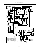
1. CONTROL BOARD (Component Side) 4. MAIN BOARD (Solder Side) 2. CONTROL BOARD (Solder Side) PRINTED CIRCUIT BOARD 3.
P/NO : 3828TSL109G Dec 2004 Printed in China