
User's Guide


Copyright ⓒ. 2017. All Rights Reserved.
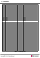
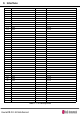
3. Interface
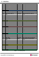
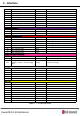
Table 1. Pin descriptions
Y7
COEX_UART_RX
* Input
LTE receiver sync for coexistence with UART
Z6
COEX_UART_TX
** Output
LTE transmitter sync for coexistence with UART
X4
RFCLK2_QCA
Output
Low noise RF clock Output
AA3
WLAN_EN_DSRC
Output
WLAN DSRC Enable
X6
DSRC_SLP_CLK
Output
DSRC sleep clock
Y5
WLAN_3V_EN_DSRC
Output
Used for WLAN enable
Z4
DSRC_PPS
** Input/Output
Pulse Per Second
X8
MDM2AP_INT_N
** Output
MDM to AP interrupt
Z8
AP2MDM_INT_N
Input
AP to MDM interrupt
Control Pin Description
A3
LGA_PHONE_ON_N
Input
ON/OFF Control
B4
MDM_RESOUT_N
Output
Reset Output
C3
LGA_RESIN_N
Input
External Reset Input
Power Supply Pin Description
A17
VPH_PWR for PAM
Input
power supply (4.0V)
B16
VPH_PWR for PAM
Input
power
supply (4.0V)
A15
VPH_PWR for PAM
Input
power
supply (4.0V)
B14
VPH_PWR for PAM
Input
power
supply (4.0V)
A9
VPH_PWR for PMIC
Input
power
supply (4.0V)
B8
VPH_PWR for PMIC
Input
power
supply (4.0V)
A7
VPH_PWR for PMIC
Input
power
supply (4.0V)
C7
VPH_PWR for PMIC
Input
power
supply (4.0V)
Voltage Reference Pin Description
C9
VREG_L11_1P8
Output
LDO out for 1.8V pull up
D8
VREG_L11_1P8
Output
LDO out for 1.8V pull up
AE3
Voltage Reference for SGMII
(VREG_L5_UIM2)
– Ethernet IO전압
level
Output
Ethernet I/O voltage
NC Pads
G9
NC
No Connect
B12
NC
No Connect
I9
NC
No Connect
G7
NC
No Connect
C5
NC
No Connect
D4
NC
No Connect
GND Pads
A21
GND
Ground
E21
GND
Ground
G21
GND
Ground
I21
GND
Ground
K21
GND
Ground
M21
GND
Ground
O21
GND
Ground
Q21
GND
Ground
S21
GND
Ground
U21
GND
Ground