
Installation Manual


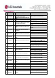
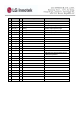


No.
Pin Name I/O
Pad Type Description
1 GND I - Ground
2 UART_RTS O
Bidirectional CMOS output, tri-state,
with weak internal pull-up
UART request to send active low
3 UART_CTS I
CMOS input with
weak internal pull
-
down
UART clear to send active low
4 UART_Rx I
CMOS input with weak internal pull
-
down
UART data input
5 UART_Tx O
Bidirectional CMOS output, tri-state,
with weak internal pull-up
UART data output
- Recommended external 4.7kΩ
ΩΩ
Ω Pull-up
resistor.
6 PCM_IN I
CMOS input, with weak internal pull-
down
Synchronous data input
-
The same pin as the I2S interface :
SD_IN
7 PCM_OUT O
CMOS output, with weak internal
pull-down
Synchronous data output
-
The same pin as the I2S interfa
ce :
SD_OUT
8 PCM_SYNC
I/O
Bidirectional with weak internal pull-
down
Synchronous data Sync
- The same pin as the I2S interface : WS
9 PCM_CLK I/O
Bidirectional with weak internal pull-
down
Synchronous data clock
- The same pin as the I2S interface : SCK
10 RESET# I
CMOS input with weak internal pull-
up
Reset if low. Input debounced so must be
low for >5ms to cause a reset
Recommended external 4.7kΩ
ΩΩ
Ω Pull-up
resistor & stability capacitor
11 VDD_3V3 I VDD
Positive supply for Module
- Supply voltage : Typical 3.3V.
12 GND I - Ground
13 SPI_MISO O
CMOS output, tristate, with weak
internal pull-down
SPI data output
- Used to program and configure (PS
Keys), and debug the BC5-MM
14 SPI_CSB I/O
Input with weak internal pull-up
Chip select for SPI, active low
- Used to program and configure (PS
Keys), and debug the BC5-MM
15 SPI_CLK I/O
Input with weak internal pull-down
SPI clock
- Used to program and configure (PS
Keys), and debug the BC5-MM
16 SPI_MOSI I
CMOS input, with weak internal pull-
down
SPI data input
- Used to program and configure (PS
Keys), and debug the BC5-MM
17 LED[1] O - LED
18 LED[0] O - LED
19 GND I - Ground
20 AGND - - Analog Ground
21 MIC_A_P I Analog Microphone input positive, left
22 MIC_A_N I Analog
Microphone input negative, left
- Must be use external ESD protection
PIN Descriptions