
Users Manual Part 1


Page 12 of 21
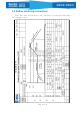
H=1.0mm,W=1.0mm,D=0.254mm(recommended)
H=1.2mm,W=1.0mm,D=0.2mm(recommended)
H=1.6mm,W=1.0mm,D=0.2mm (recommended)
(More design support is available to Lierda Technology Consulting)
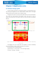
4.2Backplanelayoutconsiderations
A large clearance area is required around the antenna. Clearance refers to the open
area in the projected area of the vertical plane of the antenna (both upper and lower ranges
must be considered). In the range of the projection area of the antenna, whether it is patch
or side-insertion, do not lay the ground (especially the on-board antenna), do not have
metal or devices, and keep the antenna clearance to improve the radiation efficiency of the
antenna.
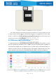
The height (distance) between the antenna and the motherboard is also an important
consideration. In general, the antenna needs to be at least 10mm above the main board, and
at least 5mm in extreme environments. When the height of the antenna is less than 8 mm,
the radiation efficiency of the antenna is limited.
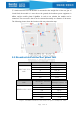
The RF part of the module should not be avoided by the metal cavity. The distance
between the RF part and the interference source should be more than 10mm. Common
sources of interference are: battery (including electrical connection), capacitor, inductor,
button, oscillator, power cord, Metal-containing screws or nuts, CPU, LCD, transformer,
speaker, camera, product communication interface cable, power circuit, motor, etc.
If the PCB antenna is used, the PCB antenna should be on the edge of the PCB on the
entire substrate. The spacing around the PCB antenna should be 10mm. The layers around
the antenna should not be copper, trace or arranged. If there are multiple antennas, the
distance between the antennas should be as far as possible to avoid co-channel interference
and intermodulation interference;
Users should pay attention to the design. In the area where the Bottom layer has
window opening for the antenna pad, no via hole can be placed to prevent short circuit.