
Datasheet

LTC2450
14
2450fb
APPLICATIONS INFORMATION
Digital Signal Levels
The LTC2450’s digital interface is easy to use. Its digital
inputs (SCK and CS) accept standard CMOS logic levels
and the internal hysteresis receivers can tolerate edge
rates as slow as 100μs. However, some considerations
are required to take advantage of the exceptional accuracy
and low supply current of this converter.
The digital output signal SDO is less of a concern because
it is not active during the conversion cycle.
While a digital input signal is in the range 0.5V to V
CC
–0.5V, the CMOS input receiver may draw additional
current from the power supply. Due to the nature of CMOS
logic, a slow transition within this voltage range may cause
an increase in the power supply current drawn by the
converter, particularly in the low power operation mode
within the SLEEP state. Thus, for low power consumption
it is highly desirable to provide relatively fast edges for the
two digital input pins SCK and CS, and to keep the digital
input logic levels at V
CC
or GND.
At the same time, during the CONVERT state, undershoot
and/or overshoot of fast digital signals connected to the
LTC2450 pins may alter the conversion result. Under-
shoot and overshoot can occur because of an impedance
mismatch at the converter pin combined with very fast
transition times. This problem becomes particularly diffi cult
when shared control lines are used and multiple refl ec-
tions may occur. The solution is to carefully terminate all
transmission lines close to their characteristic impedance.
Parallel termination is seldom an acceptable option in low
power systems so a series resistor between 27Ω and 56Ω
placed near the driver may eliminate this problem. The
actual resistor value depends upon the trace impedance
and connection topology. An alternate solution is to reduce
the edge rate of the control signals, keeping in mind the
concerns regarding slow edges mentioned above.
Particular attention should be given to confi gurations in
which a continuous clock signal is applied to SCK pin during
the CONVERT state. While LTC2450 will ignore this signal
from a logic point of view the signal edges may create
unexpected errors depending upon the relation between
its frequency and the internal oscillator frequency. In such
a situation it is benefi cial to use edge rates of about 10ns
and to limit potential undershoot to less than 0.3V below
GND and overshoot to less than 0.3V above V
CC
.
Noisy external circuitry can potentially impact the output
under 2-wire operation. In particular, it is possible to get
the LTC2450 into an unknown state if an SCK pulse is
missed or noise triggers an extra SCK pulse. In this situ-
ation, it is impossible to distinguish SDO = 1 (indicating
conversion in progress) from valid “1” data bits. As such,
CPOL = 1 is recommended for the 2-wire mode. The user
should look for SDO = 0 before reading data, and look
for SDO = 1 after reading data. If SDO does not return a
“0” within the maximum conversion time (or return a “1”
after a full data read), generate 16 SCK pulses to force a
new conversion.
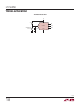
Driving V
CC
and GND
The V
CC
and GND pins of the LTC2450 converter are
directly connected to the positive and negative reference
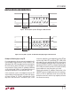
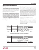
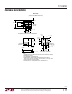
voltages, respectively. A simplifi ed equivalent circuit is
shown in Figure 14.
The power supply current passing through the parasitic
layout resistance associated with these common pins will
modify the ADC reference voltage and thus negatively affect
the converter accuracy. It is thus important to keep the
V
CC
and GND lines quiet, and to connect these supplies
through very low impedance traces.
In relation to the V
CC
and GND pins, the LTC2450 com-
bines internal high frequency decoupling with damping
Figure 14. LTC2450 Analog Pins Equivalent Circuit
V
CC
I
LEAK
R
SW
(TYP)
15k
C
EQ
(TYP)
0.35pF
INTERNAL SWITCHING FREQUENCY = 4 MHz
R
SW
(TYP)
15k
R
SW
(TYP)
15k
V
IN
I
LEAK
I
LEAK
GND
I
LEAK
V
CC
V
CC
V
CC
2450 F14