
Datasheet

LTC2450
15
2450fb
APPLICATIONS INFORMATION
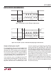
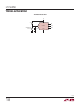
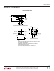
Figure 15. LTC2450 Input Drive Equivalent Circuit
elements which reduce the ADC performance sensitivity to
PCB layout and external components. Nevertheless, the very
high accuracy of this converter is best preserved by careful
low and high frequency power supply decoupling.
A 0.1μF, high quality, ceramic capacitor in parallel with a
10μF ceramic capacitor should be connected between the
V
CC
and GND pins, as close as possible to the package.
The 0.1μF capacitor should be placed closest to the ADC
package. It is also desirable to avoid any via in the circuit
path starting from the converter V
CC
pin, passing through
these two decoupling capacitors and returning to the
converter GND pin. The area encompassed by this circuit
path, as well as the path length, should be minimized.
Very low impedance ground and power planes and star
connections at both V
CC
and GND pins are preferable. The
V
CC
pin should have two distinct connections: the fi rst to the
decoupling capacitors described above and the second to
the power supply voltage. The GND pin should have three
distinct connections: the fi rst to the decoupling capacitors
described above, the second to the ground return for the
input signal source and the third to the ground return for
the power supply voltage source.
Driving V
IN
The V
IN
input drive requirements can be best analyzed
using the equivalent circuit of Figure 15. The input signal
V
SIG
is connected to the ADC input pin V
IN
through an
equivalent source resistance R
S
. This resistor includes
both the actual generator source resistance and any
additional optional resistor connected to the V
IN
pin. An
optional input capacitor C
IN
is also connected to the ADC
V
IN
pin. This capacitor is placed in parallel with the ADC
input parasitic capacitance C
PAR
. Depending upon the PCB
layout C
PAR
has typical values between 2pF and 15pF. In
addition, the equivalent circuit of Figure 15 includes the
converter equivalent internal resistor R
SW
and sampling
capacitor C
EQ
.
There are some immediate trade-offs in R
S
and C
IN
without
needing a full circuit analysis. Increasing R
S
and C
IN
can
give the following benefi ts:
1) Due to the LTC2450’s input sampling algorithm, the
input current drawn by V
IN
over a conversion cycle is
50nA. A high R
S
•
C
IN
attenuates the high frequency
components of the input current, and R
S
values up to
1kΩ result in <1LSB error.
2) The bandwidth from V
SIG
is reduced at V
IN
.This band-
width reduction isolates the ADC from high frequency
signals, and as such provides simple antialiasing and
input noise reduction.
3) Noise generated by the ADC is attenuated before it goes
back to the signal source.
4) A large C
IN
gives a better AC ground at V
IN
, helping
reduce refl ections back to the signal source.
5) Increasing R
S
protects the ADC by limiting the current
during an outside-the-rails fault condition. R
S
can be
easily sized such as to protect against even extreme
fault conditions.
There is a limit to how large R
S
• C
IN
should be for a given
application. Increasing R
S
beyond a given point increases
the voltage drop across R
S
due to the input current, to
the point that signifi cant measurement errors exist. Ad-
ditionally, for some applications, increasing the R
S
• C
IN
product too much may unacceptably attenuate the signal
at frequencies of interest.
C
EQ
0.35pF
(TYP)
R
SW
15k
(TYP)
I
LEAK
I
LEAK
V
CC
R
S
C
IN
V
SIG
C
PAR
V
CC
I
CONV
2450 F15
V
IN
+
–