
Datasheet

LTC2450
16
2450fb
APPLICATIONS INFORMATION
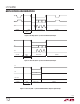
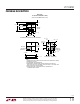
Figure 16. Measured INL vs Input Voltage,
C
IN
= 0.1μF, V
CC
= 5V, T
A
= 25°C
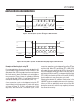
For most applications, it is desirable to implement C
IN
as
a high quality 0.1μF ceramic capacitor and R
S
≤ 1k. This
capacitor should be located as close as possible to the
actual V
IN
package pin. Furthermore the area encompassed
by this circuit path as well as the path length should be
minimized.
In the case of a 2-wire sensor which is not remotely
grounded, it is desirable to split R
S
and place series
resistors in the ADC input line as well as in the sensor
ground return line which should be tied to the ADC GND
pin using a star connection topology.
Figure 16 shows the measured LTC2450 INL vs In-
put Voltage as a function of R
S
value with an input
capacitor C
IN
= 0.1μF.
In some cases, R
S
can be increased above these guidelines.
In the case of the LTC2450, in the fi rst half of the CONVERT
state, the internal calibration algorithm maintains I
AV
strictly at zero. Each half of the CONVERT state is about
16.67ms. Additionally, the input current is zero while the
ADC is either in sleep or I/O modes. Thus, if the time
constant of the input R-C circuit τ = R
S
• C
IN
is of the
same order magnitude or longer than the time periods
between actual conversions, then one can consider the
input current to be reduced correspondingly.
These considerations need to be balanced out by the input
signal bandwidth. The 3dB bandwidth ≅ 1/(2π R
S
C
IN
).
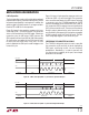
Finally, if the recommended choice for C
IN
is unacceptable
for the user’s specifi c application, an alternate strategy is to
eliminate C
IN
and minimize C
PAR
and R
S
. In practical terms,
this confi guration corresponds to a low impedance sensor
directly connected to the ADC through minimum length
traces. Actual applications include current measurements
through low value sense resistors, temperature measure-
ments, low impedance voltage source monitoring and so
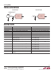
on. The resultant INL vs V
IN
is shown in Figure 17. The
measurements of Figure 17 include a C
PAR
capacitor cor-
responding to a minimum size layout pad and a minimum
width input trace of about 1 inch length.
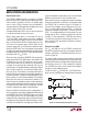
Figure 17. Measured INL vs V
IN
, C
IN
= 0, V
CC
= 5V, T
A
= 25°C
INPUT VOLTAGE (V)
0
INL(LSB)
–4
0
4
3
5
2450 F16
–8
–12
–16
12 4
8
12
16
R
S
= 10k
R
S
= 1k
R
S
= 0
INPUT VOLTAGE (V)
0
INL (LSB)
8
6
4
2
0
–2
–4
–6
–8
4
2450 F17
123 53.50.5 1.5 2.5 4.5
R
S
= 1k
R
S
= 10k
R
S
= 0