
Datasheet

LTC2450
3
2450fb
Note 1: Stresses beyond those listed under Absolute Maximum Ratings
may cause permanent damage to the device. Exposure to any Absolute
Maximum Rating condition for extended periods may affect device
reliability and lifetime.
Note 2: All voltage values are with respect to GND. V
CC
= 2.7V to 5.5V
unless otherwise specifi ed.
Note 3: Guaranteed by design, not subject to test.
Note 4: Integral nonlinearity is defi ned as the deviation of a code from
a straight line passing through the actual endpoints of the transfer
curve. The deviation is measured from the center of the quantization
band. Guaranteed by design, test correlation and 3 point transfer curve
measurement.
SYMBOL PARAMETER CONDITIONS MIN TYP MAX UNITS
V
CC
Supply Voltage
l
2.7 5.5 V
I
CC
Supply Current
Conversion
Sleep
CS = GND (Note 6)
CS = VCC (Note 6)
l
l
350
0.05
600
0.5
μA
μA
The l denotes the specifi cations which apply over the full
operating temperature range,otherwise specifi cations are at T
A
= 25°C. (Note 2)
POWER REQUIREMENTS
SYMBOL PARAMETER CONDITIONS MIN TYP MAX UNITS
V
IH
High Level Input Voltage
l
V
CC
– 0.3 V
V
IL
Low Level Input Voltage
l
0.3 V
I
IN
Digital Input Current
l
–10 10 μA
C
IN
Digital Input Capacitance 10 pF
V
OH
High Level Output Voltage I
O
= –800μA
l
V
CC
– 0.5 V
V
OL
Low Level Output Voltage I
O
= –1.6mA
l
0.4 V
I
OZ
Hi-Z Output Leakage Current
l
–10 10 μA
The l denotes the specifi cations which apply over the full operating temperature
range,otherwise specifi cations are at T
A
= 25°C.
The l denotes the specifi cations which apply over the full operating temperature
range,otherwise specifi cations are at T
A
= 25°C.
SYMBOL PARAMETER CONDITIONS MIN TYP MAX UNITS
t
CONV
Conversion Time
l
29 33.3 42 ms
f
SCK
SCK Frequency Range
l
2 MHz
t
lSCK
SCK Low Period
l
250 ns
t
hSCK
SCK High Period
l
250 ns
t
1
CS Falling Edge to SDO Low Z (Notes 7, 8)
l
0100ns
t
2
CS Rising Edge to SDO High Z (Notes 7, 8)
l
0100ns
t
3
CS Falling Edge to SCK Falling Edge
l
100 ns
t
KQ
SCK Falling Edge to SDO Valid (Note 7)
l
0100ns
Note 5: CS = V
CC
. A positive current is fl owing into the DUT pin.
Note 6: SCK = V
CC
or GND. SDO is high impedance.
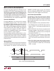
Note 7: See Figure 3.
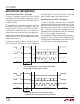
Note 8: See Figure 4.
Note 9: Input sampling current is the average input current drawn from the
input sampling network while the LTC2450 is actively sampling the input.
DIGITAL INPUTS AND DIGITAL OUTPUTS
TIMING CHARACTERISTICS