
Datasheet

LTC2450
6
2450fb
PIN FUNCTIONS
V
CC
(Pin 1): Positive Supply Voltage and Converter Refer-
ence Voltage. Bypass to GND (Pin 3) with a 10μF capacitor
in parallel with a low series inductance 0.1μF capacitor
located as close to the part as possible.
V
IN
(Pin 2): Analog Input Voltage.
GND (Pin 3): Ground. Connect to a ground plane through
a low impedance connection.
CS (Pin 4): Chip Select Active LOW Digital Input. A LOW on
this pin enables the SDO digital output. A HIGH on this pin
places the SDO output pin in a high impedance state.
SDO (Pin 5): Three-State Serial Data Output. SDO is used
for serial data output during the DATA OUTPUT state and
can be used to monitor the conversion status.
SCK (Pin 6): Serial Clock Input. SCK synchronizes the serial
data output. While digital data is available (the ADC is not
in CONVERT state) and CS is LOW (ADC is not in SLEEP
state) a new data bit is produced at the SDO output pin
following every falling edge applied to the SCK pin.
Exposed Pad (Pin 7): Ground. The Exposed Pad must be
soldered to the same point as Pin 3.
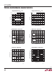
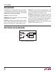
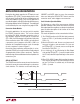
Figure 1. Functional Block Diagram
FUNCTIONAL BLOCK DIAGRAM
SPI
INTERFACE
16 BIT ΔΣ
A/D
CONVERTER
INTERNAL
OSCILLATOR
REF +
CS
SDO
SCK
GND
V
IN
V
CC
V
CC
REF –
2450 BD