
Datasheet

LTC2450
7
2450fb
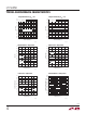
CONVERTER OPERATION
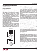
Converter Operation Cycle
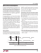
The LTC2450 is a low power, delta-sigma analog-to-
digital converter with a simple 3-wire interface (see
Figure 1). Its operation is composed of three successive
states: CONVERT, SLEEP and DATA OUTPUT. The operat-
ing cycle begins with the CONVERT state, is followed
by the SLEEP state and ends with the DATA OUTPUT
state (see Figure 2). The 3-wire interface consists of
serial data output (SDO), serial clock input (SCK) and the
active low chip select input (CS).
The CONVERT state duration is determined by the LTC2450
conversion time (nominally 33.3 milliseconds). Once
started, this operation can not be aborted except by a low
power supply condition (V
CC
< 2.1V) which generates an
internal power-on reset signal.
After the completion of a conversion, the LTC2450 enters
the SLEEP state and remains here until both the chip
select and clock inputs are low (CS = SCK = LOW). Fol-
lowing this condition the ADC transitions into the DATA
OUTPUT state.
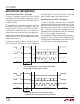
Figure 2. LTC2450 State Transition Diagram
APPLICATIONS INFORMATION
While in the SLEEP state, whenever the chip select input
is pulled high (CS = HIGH), the LTC2450’s power supply
current is reduced to less than 200nA. When the chip select
input is pulled low (CS = LOW), and SCK is maintained
at a HIGH logic level, the LTC2450 will return to a normal
power consumption level. During the SLEEP state, the
result of the last conversion is held indefi nitely in a static
register.
Upon entering the DATA OUTPUT state, SDO outputs the
most signifi cant bit (D15) of the conversion result. During
this state, the ADC shifts the conversion result serially
through the SDO output pin under the control of the SCK
input pin. There is no latency in generating this result and
it corresponds to the last completed conversion. A new
bit of data appears at the SDO pin following each falling
edge detected at the SCK input pin. The user can reliably
latch this data on every rising edge of the external serial
clock signal driving the SCK pin (see Figure 3).
The DATA OUTPUT state concludes in one of two dif-
ferent ways. First, the DATA OUTPUT state operation is
completed once all 16 data bits have been shifted out and
the clock then goes low, which corresponds to the 16
th
falling edge of SCK. Second, the DATA OUTPUT state can
be aborted at any time by a LOW-to-HIGH transition on
the CS input. Following either one of these two actions,
the LTC2450 will enter the CONVERT state and initiate a
new conversion cycle.
Power-Up Sequence
When the power supply voltage V
CC
applied to the con-
verter is below approximately 2.1V, the ADC performs a
power-on reset. This feature guarantees the integrity of
the conversion result.
When V
CC
rises above this critical threshold, the converter
generates an internal power-on reset (POR) signal for
approximately 0.5ms. The POR signal clears all internal
registers. Following the POR signal, the LTC2450 starts
a conversion cycle and follows the succession of states
described in Figure 2. The fi rst conversion result fol-
lowing POR is accurate within the specifi cations of the
device if the power supply voltage V
CC
is restored within
the operating range (2.7V to 5.5V) before the end of the
POR time interval.
DATA OUTPUT
SLEEP
CONVERT
POWER-ON RESET
YES
2450 F02
16TH FALLING
EDGE OF SCK
OR
CS = HIGH?
SCK = LOW
AND
CS = LOW?
NO YES
NO