
Datasheet

LTC2450
8
2450fb
APPLICATIONS INFORMATION
this range. Thus the converter resolution remains at 1LSB
independent of the reference voltage. INL, offset, and full-
scale errors vary with the reference voltage as indicated
by the Typical Performance Characteristics graphs. These
error terms will decrease with an increase in the reference
voltage (as the LSB size in μV increases).
Input Voltage Range
The ADC is capable of digitizing true rail-to-rail input sig-
nals. Ignoring offset and full-scale errors, the converter
will theoretically output an “all zero” digital result when the
input is at ground (a zero scale input) and an “all one” digital
result when the input is at V
CC
(a full-scale input).
The converter offset and gain error specifi cations ensure
that all 65536 possible codes will be produced within this
voltage range. In an under-range condition, for all input
voltages less than the voltage corresponding to output
code 0, the converter will generate the output code 0.
In an over-range condition, for all input voltages greater
than the voltage corresponding to output code 65535 the
converter will generate the output code 65535.
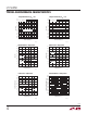
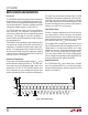
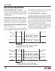
Output Data Format
The LTC2450 generates a 16-bit direct binary encoded
result. It is provided, MSB fi rst, as a 16-bit serial stream
through the SDO output pin under the control of the SCK
input pin (see Figure 3).
Ease of Use
The LTC2450 data output has no latency, fi lter settling delay
or redundant results associated with the conversion cycle.
There is a one-to-one correspondence between the conver-
sion and the output data. Therefore, multiplexing multiple
analog input voltages requires no special actions.
The LTC2450 performs offset and full-scale calibrations
every conversion. This calibration is transparent to the
user and has no effect upon the cyclic operation described
previously. The advantage of continuous calibration is
extreme stability of the ADC performance with respect to
time and temperature.
The LTC2450 includes a proprietary input sampling scheme
that reduces the average input current several orders of
magnitude as compared to traditional delta sigma archi-
tectures. This allows external fi lter networks to interface
directly to the LTC2450. Since the average input sampling
current is 50nA, an external RC lowpass fi lter using a 1kΩ
and 0.1μF results in <1LSB error.
Reference Voltage Range
The converter uses the power supply voltage (V
CC
) as the
positive reference voltage (see Figure 1). Thus, the refer-
ence range is the same as the power supply range, which
extends from 2.7V to 5.5V. The LTC2450’s internal noise
level is extremely low so the output peak-to-peak noise
remains well below 1LSB for any reference voltage within
Figure 3. Data Output Timing
D
15
LSB
SDO
SCK
D
14
D
13
D
12
D
11
D
10
D
9
D
8
D
7
D
6
D
5
D
4
D
3
D
2
D
0
D
1
2450 F02
t
1
t
3
t
KQ
t
lSCK
t
hSCK
t
2
CS
MSB