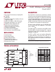
LTC2188 16-Bit, 20Msps Low Power Dual ADC Features n n n n n n n n n n n n n Description Two-Channel Simultaneously Sampling ADC 77dB SNR 90dB SFDR Low Power: 76mW Total, 38mW per Channel Single 1.
LTC2188 Absolute Maximum Ratings (Notes 1, 2) Supply Voltages (VDD, OVDD)........................ –0.3V to 2V Analog Input Voltage (AIN+, AIN –, PAR/SER, SENSE) (Note 3)........... –0.3V to (VDD + 0.2V) Digital Input Voltage (ENC+, ENC–, CS, SDI, SCK) (Note 4)..................................... –0.3V to 3.9V SDO (Note 4).............................................. –0.3V to 3.9V Digital Output Voltage................. –0.3V to (OVDD + 0.3V) Operating Temperature Range LTC2188C.........................
LTC2188 Pin ConfigurationS DOUBLE DATA RATE LVDS OUTPUT MODE 64 VDD 63 SENSE 62 VREF 61 SDO 60 OF2_1+ 59 OF2_1– 58 D1_14_15+ 57 D1_14_15– 56 D1_12_13+ 55 D1_12_13– 54 D1_10_11+ 53 D1_10_11– 52 D1_8_9+ 51 D1_8_9– 50 D1_6_7+ 49 D1_6_7– TOP VIEW VDD 1 VCM1 2 GND 3 AIN1+ 4 AIN1– 5 GND 6 REFH 7 REFL 8 REFH 9 REFL 10 PAR/SER 11 AIN2+ 12 AIN2– 13 GND 14 VCM2 15 VDD 16 48 D1_4_5+ 47 D1_4_5– 46 D1_2_3+ 45 D1_2_3– 44 D1_0_1+ 43 D1_0_1– 42 OVDD 41 OGND 40 CLKOUT+ 39 CLKOUT– 38 D2_14_15+ 37 D2_14_15– 36 D2_12_13+ 35
LTC2188 Converter Characteristics The l denotes the specifications which apply over the full operating temperature range, otherwise specifications are at TA = 25°C. (Note 5) PARAMETER CONDITIONS Resolution (No Missing Codes) MIN l 16 TYP MAX UNITS Bits Integral Linearity Error Differential Analog Input (Note 6) l –6.5 ±2 6.5 LSB Differential Linearity Error Differential Analog Input l –0.9 ±0.5 0.9 LSB Offset Error (Note 7) l –7 ±1.
LTC2188 Dynamic Accuracy The l denotes the specifications which apply over the full operating temperature range, otherwise specifications are at TA = 25°C. AIN = –1dBFS.
LTC2188 Digital Inputs and Outputs The l denotes the specifications which apply over the full operating temperature range, otherwise specifications are at TA = 25°C. (Note 5) SYMBOL PARAMETER CONDITIONS MIN TYP MAX UNITS ENCODE INPUTS (ENC+, ENC– ) Differential Encode Mode (ENC– Not Tied to GND) VID Differential Input Voltage (Note 8) l 0.2 VICM Common Mode Input Voltage Internally Set Externally Set (Note 8) l 1.1 l 0.2 V 1.2 1.6 V V 3.
LTC2188 Power Requirements The l denotes the specifications which apply over the full operating temperature range, otherwise specifications are at TA = 25°C. (Note 9) SYMBOL PARAMETER CONDITIONS MIN TYP MAX UNITS CMOS Output Modes: Full Data Rate and Double Data Rate VDD Analog Supply Voltage (Note 10) l 1.7 1.8 1.9 OVDD Output Supply Voltage (Note 10) l 1.1 1.8 1.
LTC2188 timing characteristics The l denotes the specifications which apply over the full operating temperature range, otherwise specifications are at TA = 25°C. (Note 5) SYMBOL PARAMETER CONDITIONS MIN TYP MAX UNITS Digital Data Outputs (LVDS Mode) tD ENC to Data Delay CL = 5pF (Note 8) l 1.1 1.8 3.2 ns tC ENC to CLKOUT Delay CL = 5pF (Note 8) l 1 1.5 2.7 ns tSKEW DATA to CLKOUT Skew tD – tC (Note 8) l 0 0.3 0.6 ns Pipeline Latency 6.
LTC2188 Timing Diagrams Full-Rate CMOS Output Mode Timing All Outputs Are Single-Ended and Have CMOS Levels tAP CH 1 ANALOG INPUT A+3 tAP CH 2 ANALOG INPUT A+4 A+2 A A+1 B+4 B+2 B B+3 tH tL B+1 ENC– ENC+ tD D1_0 - D1_15, OF1 A–6 A–5 A–4 A–3 A–2 D2_0 - D2_15, OF2 B–6 B–5 B–4 B–3 B–2 CLKOUT + CLKOUT – tC 2188 TD01 2188f 9
LTC2188 timing DIAGRAMS Double Data Rate CMOS Output Mode Timing All Outputs Are Single-Ended and Have CMOS Levels tAP CH 1 ANALOG INPUT A+3 tAP CH 2 ANALOG INPUT A+4 A+2 A A+1 B+4 B+2 B B+3 tH tL B+1 ENC– ENC+ tD tD BIT 0 A-6 BIT 1 A-6 BIT 0 A-5 BIT 1 A-5 BIT 0 A-4 BIT 1 A-4 BIT 0 A-3 BIT 1 A-3 BIT 0 A-2 D1_14_15 BIT 14 A-6 BIT 15 A-6 BIT 14 A-5 BIT 15 A-5 BIT 14 A-4 BIT 15 A-4 BIT 14 A-3 BIT 15 A-3 BIT 14 A-2 D2_0_1 BIT 0 B-6 BIT 1 B-6 BIT 0 B-5 BIT 1 B-5 BIT 0 B-4 B
LTC2188 timing DIAGRAMS Double Data Rate LVDS Output Mode Timing All Outputs Are Differential and Have LVDS Levels tAP CH 1 ANALOG INPUT A+3 tAP CH 2 ANALOG INPUT A+4 A+2 A A+1 B+4 B+2 B B+3 tH tL B+1 ENC– ENC+ D1_0_1+ D1_0_1– •• • D1_14_15+ D1_14_15– D2_0_1+ D2_0_1– •• • D2_14_15+ D2_14_15– OF2_1+ OF2_1– CLKOUT+ CLKOUT – tD tD BIT 0 A-6 BIT 1 A-6 BIT 0 A-5 BIT 1 A-5 BIT 0 A-4 BIT 1 A-4 BIT 0 A-3 BIT 1 A-3 BIT 0 A-2 BIT 14 A-6 BIT 15 A-6 BIT 14 A-5 BIT 15 A-5 BIT 14 A-4 BIT
LTC2188 timing DIAGRAMS SPI Port Timing (Readback Mode) tDS tS tDH tSCK tH CS SCK tDO SDI SDO R/W A6 A5 A4 A3 A2 A1 A0 XX D7 HIGH IMPEDANCE XX D6 XX D5 XX D4 XX D3 XX D2 XX XX D1 D0 SPI Port Timing (Write Mode) CS SCK SDI SDO R/W HIGH IMPEDANCE A6 A5 A4 A3 A2 A1 A0 D7 D6 D5 D4 D3 D2 D1 D0 2188 TD04 2188f 12
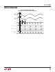
LTC2188 Typical Performance Characteristics Integral Non-Linearity (INL) 10000 3.0 0.8 9000 0.6 8000 0.4 7000 0.2 6000 DNL ERROR (LSB) INL ERROR (LSB) 1.0 0 –1.0 –2.0 –3.0 –4.0 0 16384 32768 49152 OUTPUT CODE 0 4000 –0.4 3000 –0.6 2000 –0.
LTC2188 Typical Performance Characteristics IOVDD vs Sample Rate, 5MHz, –1dBFS, Sine Wave Input on Each Channel 78 3.5mA LVDS 70 77 60 76 50 SNR (dBFS) IOVDD (mA) 80 SNR vs SENSE, fIN = 5MHz, –1dBFS 1.75mA LVDS 40 30 74 73 72 20 10 0 75 71 1.8V CMOS 0 4 8 12 16 SAMPLE RATE (Msps) 20 2188 G09 70 0.6 0.7 0.8 0.9 1 1.1 SENSE PIN (V) 1.2 1.
LTC2188 Pin Functions Pins that are the same for all Digital Output Modes VDD (Pins 1, 16, 17, 64): Analog Power Supply, 1.7V to 1.9V. Bypass to ground with 0.1µF ceramic capacitors. Adjacent pins can share a bypass capacitor. VCM1 (Pin 2): Common Mode Bias Output, nominally equal to VDD/2. VCM1 should be used to bias the common mode of the analog inputs to channel 1. Bypass to ground with a 0.1µF ceramic capacitor. GND (Pins 3, 6, 14): ADC Power Ground.
LTC2188 Pin Functions SENSE (Pin 63): Reference Programming Pin. Connecting SENSE to VDD selects the internal reference and a ±1V input range. Connecting SENSE to ground selects the internal reference and a ±0.5V input range. An external reference between 0.625V and 1.3V applied to SENSE selects an input range of ±0.8 • VSENSE. Ground (Exposed Pad Pin 65): The exposed pad must be soldered to the PCB ground.
LTC2188 Pin Functions DOUBLE DATA RATE LVDS OUTPUT MODE All Pins Below Have LVDS Output Levels. The Output Current Level Is Programmable. There Is an Optional Internal 100Ω Termination Resistor Between the Pins of Each LVDS Output Pair. D2_0_1–/D2_0_1+ to D2_14_15–/D2_14_15+ (Pins 23/24, 25/26, 27/28, 29/30, 31/32, 33/34, 35/36, 37/38): Channel 2 Double Data Rate Digital Outputs. Two data bits are multiplexed onto each differential output pair.
LTC2188 Functional Block Diagram OVDD CH 1 ANALOG INPUT OF1 16-BIT ADC CORE S/H OF2 CORRECTION LOGIC CH 2 ANALOG INPUT 16-BIT ADC CORE S/H D1_15 • • • D1_0 OUTPUT DRIVERS CLKOUT + CLKOUT – VREF 2.2µF D2_15 • • • D2_0 1.25V REFERENCE RANGE SELECT SENSE VCM1 0.1µF OGND REFH REF BUF VDD/2 REFL INTERNAL CLOCK SIGNALS VDD DIFF REF AMP CLOCK/DUTY CYCLE CONTROL MODE CONTROL REGISTERS VCM2 0.1µF GND REFH 0.1µF 2.2µF REFL ENC+ ENC– PAR/SER CS SCK SDI SDO 2188 F01 0.1µF Figure 1.
LTC2188 Applications Information Converter Operation The LTC2188 is a low power, two-channel, 16-bit, 20Msps A/D converter that is powered by a single 1.8V supply. The analog inputs should be driven differentially. The encode input can be driven differentially, or single ended for lower power consumption. The digital outputs can be CMOS, double data rate CMOS (to halve the number of output lines), or double data rate LVDS (to reduce digital noise in the system.
LTC2188 Applications Information Amplifier Circuits Reference Figure 7 shows the analog input being driven by a high speed differential amplifier. The output of the amplifier is AC-coupled to the A/D so the amplifier’s output common mode voltage can be optimally set to minimize distortion. The LTC2188 has an internal 1.25V voltage reference. For a 2V input range using the internal reference, connect SENSE to VDD. For a 1V input range using the internal reference, connect SENSE to ground.
LTC2188 Applications Information REFL pins are connected by short jumpers in an internal layer. To minimize the inductance of these jumpers they can be placed in a small hole in the GND plane on the second board layer. LTC2188 VREF 1.25V 5Ω 2.2µF 1.25V BANDGAP REFERENCE 0.625V TIE TO VDD FOR 2V RANGE; TIE TO GND FOR 1V RANGE; RANGE = 1.6 • VSENSE FOR 0.625V < VSENSE < 1.300V RANGE DETECT AND CONTROL SENSE BUFFER INTERNAL ADC HIGH REFERENCE C2 0.1µF – + REFH + – REFL – + REFH + – REFL 0.
LTC2188 Applications Information LTC2188 mode, ENC– should stay at least 200mV above ground to avoid falsely triggering the single ended encode mode. For good jitter performance ENC+ and ENC– should have fast rise and fall times. VDD DIFFERENTIAL COMPARATOR VDD The single-ended encode mode should be used with CMOS encode inputs. To select this mode, ENC– is connected to ground and ENC+ is driven with a square wave encode input. ENC+ can be taken above VDD (up to 3.6V) so 1.8V to 3.
LTC2188 Applications Information Full Rate CMOS Mode In full rate CMOS mode the data outputs (D1_0 to D1_15 and D2_0 to D2_15), overflow (OF2, OF1), and the data output clocks (CLKOUT+, CLKOUT–) have CMOS output levels. The outputs are powered by OVDD and OGND which are isolated from the A/D core power and ground. OVDD can range from 1.1V to 1.9V, allowing 1.2V through 1.8V CMOS logic outputs. For good performance the digital outputs should drive minimal capacitive loads.
LTC2188 Applications Information Phase Shifting the Output Clock Data Format In Full Rate CMOS mode the data output bits normally change at the same time as the falling edge of CLKOUT+, so the rising edge of CLKOUT+ can be used to latch the output data. In Double Data Rate CMOS and LVDS modes the data output bits normally change at the same time as the falling and rising edges of CLKOUT+.
LTC2188 Applications Information Digital Output Randomizer CLKOUT Interference from the A/D digital outputs is sometimes unavoidable. Digital interference may be from capacitive or inductive coupling or coupling through the ground plane. Even a tiny coupling factor can cause unwanted tones in the ADC output spectrum. By randomizing the digital output before it is transmitted off chip, these unwanted tones can be randomized which reduces the unwanted tone amplitude.
LTC2188 Applications Information Digital Output Test Patterns To allow in-circuit testing of the digital interface to the A/D, there are several test modes that force the A/D data outputs (OF, D15-D0) to known values: temperature shift caused by the change in supply current as the A/D leaves nap mode. Either channel 2 or both channels can be placed in nap mode; it is not possible to have channel 1 in nap mode and channel 2 operating normally.
LTC2188 Applications Information To use the serial programming mode, PAR/SER should be tied to ground. The CS, SCK, SDI and SDO pins become a serial interface that program the A/D mode control registers. Data is written to a register with a 16-bit serial word. Data can also be read back from a register to verify its contents. Serial data transfer starts when CS is taken low. The data on the SDI pin is latched at the first 16 rising edges of SCK. Any SCK rising edges after the first 16 are ignored.
LTC2188 Applications Information Table 3. Serial Programming Mode Register Map (PAR/SER = GND) REGISTER A0: RESET REGISTER (ADDRESS 00h) D7 D6 D5 D4 D3 D2 D1 D0 RESET X X X X X X X RESET Bit 7 Software Reset Bit 0 = Not Used 1 = Software Reset. All Mode Control Registers Are Reset to 00h. The ADC Is Momentarily Placed in SLEEP Mode. This Bit Is Automatically Set Back to Zero at the End of the SPI Write Command. The Reset Register Is Write-Only.
LTC2188 Applications Information REGISTER A3: OUTPUT MODE REGISTER (ADDRESS 03h) D7 D6 D5 D4 D3 D2 D1 D0 X ILVDS2 ILVDS1 ILVDS0 TERMON OUTOFF OUTMODE1 OUTMODE0 Bit 7 Unused, Don’t Care Bit. Bits 6-4 ILVDS2:ILVDS0 LVDS Output Current Bits 000 = 3.5mA LVDS Output Driver Current 001 = 4.0mA LVDS Output Driver Current 010 = 4.5mA LVDS Output Driver Current 011 = Not Used 100 = 3.0mA LVDS Output Driver Current 101 = 2.5mA LVDS Output Driver Current 110 = 2.
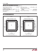
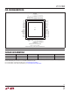
LTC2188 Typical Applications Silkscreen Top Top Side 2188f 30
LTC2188 TYPICAL APPLICATIONS Inner Layer 2 GND Inner Layer 3 2188f 31
LTC2188 TYPICAL APPLICATIONS Inner Layer 4 Inner Layer 5 Power 2188f 32
LTC2188 TYPICAL APPLICATIONS Bottom Side 2188f 33
LTC2188 TYPICAL APPLICATIONS SDO C23 2.2µF SENSE 49 D1_6_7– 51 52 53 54 55 56 57 50 D1_6_7+ D1_8_9– D1_8_9+ D1_10_11– D1_10_11+ D1_12_13– D1_12_13+ 58 PAR/SER D2_14_15+ + D2_14_15– – D2_12_13+ AIN2 AIN2 GND D2_12_13– VCM2 D2_10_11+ D2_10_11– D2_8_9+ PAD 48 DIGITAL OUTPUTS 47 46 45 44 43 42 C37 0.1µF 41 40 OVDD 39 38 37 36 35 34 33 DIGITAL OUTPUTS 65 32 31 D2_0_1 24 SDI 23 SCK 22 CS 21 20 ENC+ VDD 17 C18 0.1µF D2_8_9– VDD AIN2– C67 0.
LTC2188 Package Description UP Package 64-Lead Plastic QFN (9mm × 9mm) (Reference LTC DWG # 05-08-1705 Rev C) 0.70 ±0.05 7.15 ±0.05 7.50 REF 8.10 ±0.05 9.50 ±0.05 (4 SIDES) 7.15 ±0.05 PACKAGE OUTLINE 0.25 ±0.05 0.50 BSC RECOMMENDED SOLDER PAD PITCH AND DIMENSIONS APPLY SOLDER MASK TO AREAS THAT ARE NOT SOLDERED 9 .00 ± 0.10 (4 SIDES) 0.75 ± 0.05 R = 0.10 TYP R = 0.115 TYP 63 64 0.40 ± 0.10 PIN 1 TOP MARK (SEE NOTE 5) 1 2 PIN 1 CHAMFER C = 0.35 7.50 REF (4-SIDES) 7.15 ± 0.10 7.15 ± 0.
LTC2188 Typical Application LTC2188: Integral Non-Linearity (INL) 4.0 3.0 INL ERROR (LSB) 2.0 1.0 0 –1.0 –2.0 –3.0 –4.0 0 16384 32768 49152 OUTPUT CODE 65536 2188 TA03 Related Parts PART NUMBER DESCRIPTION COMMENTS ADCs LTC2259-14/LTC2260-14/ 14-Bit, 80Msps/105Msps/125Msps LTC2261-14 1.8V ADCs, Ultralow Power 89mW/106mW/127mW, 73.4dB SNR, 85dB SFDR, DDR LVDS/DDR CMOS/CMOS Outputs, 6mm × 6mm QFN-40 LTC2262-14 149mW, 72.