
Datasheet


LTM8028
10
8028fa
For more information www.linear.com/LTM8028
applicaTions inForMaTion
For most applications, the design process is straight
forward, summarized as follows:
1. Look at Table 1 and find the row that has the desired
input range and output voltage.
2. Apply 10μF to V
IN
and the recommended R
T
value
(R
T(OPTIMAL)
in Table 1). Lower R
T
values (resulting in
a higher operating frequency) may be used to reduce
the output ripple. Do not use values below R
T(MIN)
.
3. Apply a parallel combination of a 100μF ceramic and
a 470μF electrolytic to BKV. The Sanyo OS-CON 6SEP
-
C470M or United Chemi-Con APXF6R3ARA471MH80G
work well for the electrolytic capacitor, but other devices
with an ESR about 10mΩ may be used.
4. Apply a minimum of 37μF to V
OUT
. As shown in Table1,
this is usually a parallel combination of 4.7μF, 10μF and
22μF capacitors.
5. Apply an additional 100µF capacitor to V
OUT
if very
small (2%) transient response is required.
While these component combinations have been tested
for proper operation, it is incumbent upon the user to
verify proper operation over the intended system’s line,
load and environmental conditions. Bear in mind that the
maximum output current is limited by junction tempera
-
ture, the relationship between the input and output voltage
magnitude and polarity and other factors. Please refer to
the graphs in the T
ypical Performance Characteristics
section for guidance.
The maximum frequency (and attendant R
T
value) at
which the LTM8028 should be allowed to switch is given
in Table 1 in the f
MAX
column, while the recommended
frequency (and R
T
value) for optimal efficiency over the
given input condition is given in the f
OPTIMAL
column.
There are additional conditions that must be satisfied if
the synchronization function is used. Please refer to the
Synchronization section for details.
Programming Output Voltage
Three tri-level input pins, V
O2
, V
O1
and V
O0
, select the value
of output voltage. Table 2 illustrates the 3-bit digital word-
to-output voltage resulting from setting these pins high,
low or allowing them to float. These pins may be tied high
or low by either pin-strapping them to V
OB
or driving them
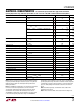
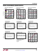
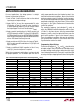
Table 1: Recommended Component Values and Configuration (T
A
= 25°C)
V
IN
V
OUT
f
OPTIMAL
R
T(OPTIMAL)
f
MAX
R
T(MIN)
6V to 36V 0.8V 200kHz 200k 250kHz 165k
6V to 36V 1.0V 250kHz 165k 280kHz 150k
6V to 36V 1.2V 250kHz 165k 315kHz 133k
6V to 36V 1.5V 250kHz 165k 333kHz 127k
6V to 36V 1.8V 315kHz 133k 385kHz 107k
9V to 15V 0.8V 250kHz 165k 650kHz 61.9k
9V to 15V 1.0V 280kHz 150k 750kHz 53.6k
9V to 15V 1.2V 300kHz 143k 800kHz 49.9k
9V to 15V 1.5V 315kHz 133k 1MHz 40.2k
9V to 15V 1.8V 350kHz 118k 1MHz 40.2k
18V to 36V 0.8V 200kHz 200k 250kHz 165k
18V to 36V 1.0V 250kHz 165k 280kHz 150k
18V to 36V 1.2V 250kHz 165k 315kHz 133k
18V to 36V 1.5V 250kHz 165k 333kHz 127k
18V to 36V 1.8V 315kHz 133k 385kHz 107k
C
IN
: 10µF, 50V, 1210
C
BKV
: 100µF, 6.3V, 1210 + 470µF, 6.3V Low ESR Electrolytic
C
OUT
: 4.7µF, 4V, 0603 + 10µF, 10V, 0805 + 22µF, 10V, 0805
C
OUT
(Optional): 100µF, 6.3V, 1210
Note: An input bulk capacitor is required.