
Datasheet
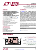


LTM8028
7
8028fa
For more information www.linear.com/LTM8028
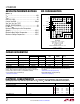
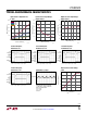
pin FuncTions
V
OUT
(Bank 1): Power Output Pins. Apply the output filter
capacitor and the output load between these and the GND
pins.
BKV (Bank 2): Buck Regulator Output. Apply the step-down
regulator’s bulk capacitance here (refer to Table 1). Do not
connect this to the load. Do not drive a voltage into BKV.
GND (Bank 3): Tie these GND pins to a local ground plane
below the LTM8028 and the circuit components. In most
applications, the bulk of the heat flow out of the LTM8028
is through these pads, so the printed circuit design has a
large impact on the thermal performance of the part. See
the PCB Layout and Thermal Considerations sections for
more details.
V
IN
(Bank 4): The V
IN
pin supplies current to the LTM8028’s
internal regulator and to the internal power switch. This
pin must be locally bypassed with an external, low ESR
capacitor; see Table 1 for recommended values.
V
O0
, V
O1
, V
O2
(Pin A6, Pin B6, Pin A5): Output Voltage
Select. These three-state pins combine to select a nominal
output voltage from 0.8V to 1.8V in increments of 50mV. See
Table 2 in the Applications Information section that defines
the V
O2
, V
O1
and V
O0
settings versus V
OUT
.
MARGA (Pin A7): Analog Margining: This pin margins the
output voltage over a continuous analog range of ±10%.
Tying this pin to GND adjusts output voltage by –10%.
Driving this pin to 1.2V adjusts output voltage by 10%. A
voltage source or a voltage output DAC is ideal for driving
this pin. If the MARGA function is not used, either float
this pin or terminate with a 1nF capacitor to GND.
TEST (Pin A8): Factory Test. Leave this pin open.
SENSEP (Pin A9): Kelvin Sense for V
OUT
. The SENSEP
pin is the inverting input to the error amplifier. Optimum
regulation is obtained when the SENSEP pin is connected
to the V
OUT
pins of the regulator. In critical applications, the
resistance of PCB traces between the regulator and the load
can cause small voltage drops, creating a load regulation
error at the point of load. Connecting the SENSEP pin at
the load instead of directly to V
OUT
eliminates this voltage
error. The SENSEP pin input bias current depends on the
selected output voltage. SENSEP pin input current varies
from 50μA typically at V
OUT
= 0.8V to 300μA typically at
V
OUT
= 1.8V. SENSEP must be connected to V
OUT
, either
locally or remotely.
V
OB
(Pin B5): Bias for V
O0
, V
O1
, V
O2
. This is a 3.3V source
to conveniently pull up the V
O0
, V
O1
, V
O2
pins, if desired.
If not used, leave this pin floating.
I
MAX
(Pin D1): Sets the Maximum Output Current. Con-
nect a resistor/ NTC thermistor network to the I
MAX
pin
to reduce the maximum regulated output current of the
LTM8028 in response to temperature. This pin is internally
pulled up to 2V through a 10k resistor, and the control
voltage range is 0V to 1.5V.
SS (Pin D2): The Soft-Start Pin. Place an external capacitor
to ground to limit the regulated current during start-up
conditions. The soft-start pin has an 11μA charging current.
RT (Pin E1): The RT pin is used to program the switching
frequency of the LTM8028’s buck regulator by connect
-
ing a resistor from this pin to ground. The Applications
Information section of the data sheet includes a table
to determine the resistance value based on the desired
switching frequency. When using the SYNC function,
set the frequency to be 20% lower than the SYNC pulse
frequency. Do not leave this pin open.
SYNC (Pin E2): Frequency Synchronization Pin. This pin
allows the switching frequency to be synchronized to an
external clock. The R
T resistor should be chosen to oper
-
ate the internal clock at 20% slower than the SYNC pulse
frequency. This pin should be grounded when not in use.
Do not leave this pin floating. When laying out the board,
avoid noise coupling to or from the SYNC trace. See the
Synchronization section in Applications Information.
RUN (Pin F1): The RUN pin acts as an enable pin and
turns off the internal circuitry at 1.55V. The pin does not
have any pull-up or pull-down, requiring a voltage bias for
normal part operation. The RUN pin is internally clamped,
so it may be pulled up to a voltage source that is higher
than the absolute maximum voltage of 6V, provided the
pin current does not exceed 100μA.