
Datasheet


LT1173
10
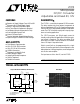
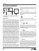
L1
LT1173 • TA13
GND SW2
FB
SW1
LIM
I
IN
V
D1
AO
+V
OUT
R2
V = 1.245V + 0.6V
OUT
R1
R2
( )
R1
2N3906
–V
IN
+
C1
LT1173
+
C2
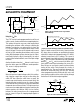
Figure 8. Negative-to-Positive Converter
Using the I
LIM
Pin
The LT1173 switch can be programmed to turn off at a set
switch current, a feature not found on competing devices.
This enables the input to vary over a wide range without
exceeding the maximum switch rating or saturating the
inductor. Consider the case where analysis shows the
LT1173 must operate at an 800mA peak switch current
with a 2.0V input. If V
IN
rises to 4V, the peak switch current
will rise to 1.6A, exceeding the maximum switch current
rating. With the proper resistor selected (see the “Maxi-
mum Switch
Current vs R
LIM
” characteristic), the switch
current will be limited to 800mA, even if the input voltage
increases.
Another situation where the I
LIM
feature is useful occurs
when the device goes into continuous mode operation.
This occurs in step-up mode when
V
V
VV DC
OUT DIODE
IN SW
+
−
<
−
()
1
1
17.
When the input and output voltages satisfy this relation-
ship, inductor current does not go to zero during the
switch OFF time. When the switch turns on again, the
current ramp starts from the non-zero current level in the
inductor just prior to switch turn on. As shown in Figure
9, the inductor current increases to a high level before the
comparator turns off the oscillator. This high current can
cause excessive output ripple and requires oversizing the
output capacitor and inductor. With the I
LIM
feature,
however, the switch current turns off at a programmed
level as shown in Figure 10, keeping output ripple to a
minimum.
U
S
A
O
PP
L
IC
AT
I
WU
U
I FOR ATIO
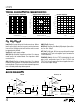
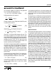
LT1173 • TA14
I
OFF
L
ON
SWITCH
Figure 9. No Current Limit Causes Large Inductor
Current Build-Up
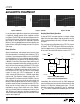
LT1173 • TA15
I
ON
L
OFF
SWITCH
PROGRAMMED CURRENT LIMIT
Figure 10. Current Limit Keeps Inductor Current Under Control
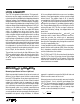
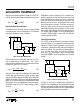
Figure 11 details current limit circuitry. Sense transistor
Q1, whose base and emitter are paralleled with power
switch Q2, is ratioed such that approximately 0.5% of Q2’s
collector current flows in Q1’s collector. This current is
passed through internal 80Ω resistor R1 and out through
the I
LIM
pin. The value of the external resistor connected
between I
LIM
and V
IN
sets the current limit. When suffi-
cient switch current flows to develop a V
BE
across R1 +
R
LIM
, Q3 turns on and injects current into the oscillator,
turning off the switch. Delay through this circuitry is
approximately 2µs. The current trip point becomes less
accurate for switch ON times less than 4µs. Resistor
values programming switch ON time for 2µs or less will
cause spurious response in the switch circuitry although
the device will still maintain output regulation.
LT1173 • TA28
SW2
SW1
Q2
DRIVER
OSCILLATOR
V
IN
I
LIM
R1
80Ω
(INTERNAL)
R
LIM
(EXTERNAL)
Q1
Q3
Figure 11. LT1173 Current Limit Circuitry