
Datasheet


LT1173
11
U
S
A
O
PP
L
IC
AT
I
WU
U
I FOR ATIO
Using the Gain Block
The gain block (GB) on the LT1173 can be used as an error
amplifier, low battery detector or linear post regulator. The
gain block itself is a very simple PNP input op amp with an
open collector NPN output. The negative input of the gain
block is tied internally to the 1.245V reference. The posi-
tive input comes out on the SET pin.
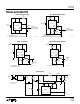
Arrangement of the gain block as a low battery detector is
straightforward. Figure 12 shows hookup. R1 and R2 need
only be low enough in value so that the bias current of the
SET input does not cause large errors. 100kΩ for R2 is
adequate. R3 can be added to introduce a small amount of
hysteresis. This will cause the gain block to “snap” when
the trip point is reached. Values in the 1M-10M range are
optimal. The addition of R3 will change the trip point,
however.
Table 1. Component Selection for Common Converters
INPUT OUTPUT OUTPUT CIRCUIT INDUCTOR INDUCTOR CAPACITOR
VOLTAGE VOLTAGE CURRENT (MIN) FIGURE VALUE PART NUMBER VALUE NOTES
2.0-3.1 5 90mA 5 47µH G GA10-472K, C CTX50-1 100µF*
2.0-3.1 5 10mA 5 220µH G GA10-223K, C CTX 22µF
2.0-3.1 12 50mA 5 47µH G GA10-472K, C CTX50-1 47µF*
2.0-3.1 12 10mA 5 150µH G GA10-153K 22µF
5 12 90mA 5 120µH G GA10-123K 100µF
5 12 30mA 5 150µH G GA10-153K 47µF**
5 15 50mA 5 120µH G GA10-123K C CTX100-4 47µF
5 30 25mA 5 100µH G GA10-103K, C CTX100-4 10µF, 50V
6.5-9.5 5 50mA 6 47µH G GA10-472K, C CTX50-1 100µF**
12-20 5 300mA 6 220µH G GA20-223K 220µF**
20-30 5 300mA 6 470µH G GA20-473K 470µF**
5 –5 75mA 7 100µH G GA10-103K, C CTX100-4 100µF**
12 –5 250mA 7 470µH G GA40-473K 220µF**
–5 5 150mA 8 100µH G GA10-103K, C CTX100-4 220µF
–5 12 75mA 8 100µH G GA10-103K, C CTX100-4 47µF
G = Gowanda
C = Coiltronics
* Add 68Ω from I
LIM
to V
IN
** Add 100Ω from I
LIM
to V
IN
LT1173 • TA16
V
BAT
R1
R2
1.245V
REF
SET
GND
IN
V
LT1173
100k
+5V
TO
PROCESSOR
R1 =
V
LB
– 1.245V
11.7µA
V
LB
+
–
AO
R3
= BATTERY TRIP POINT
R2 = 100kΩ
R3 = 4.7MΩ
Figure 12. Setting Low Battery Detector Trip Point