
Datasheet


LT1173
4
CCHARA TERIST
ICS
UW
AT
Y
P
I
CA
LPER
F
O
R
C
E
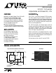
LT1173 • BD02
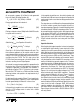
IN
V
GND
SET
AO
A2
1.245V
REFERENCE
A1
OSCILLATOR
DRIVER
R1
SW1
SW2
LIM
I
Ω
R2
753k
SENSE
LT1173-5:
LT1173-12:
R1 = 250k
R1 = 87.4k
Ω
Ω
GAIN BLOCK/
ERROR AMP
COMPARATOR
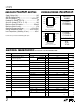
LT1173 • BD01
IN
V
GND
SET
AO
1.245V
REFERENCE
A1
A2
DRIVER
FB
SW1
SW2
LIM
I
OSCILLATOR
GAIN BLOCK/
ERROR AMP
COMPARATOR
LT1173
LT1173-5, -12
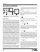
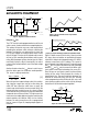
W
IDAGRA
B
L
O
C
K
S
I
LIM
(Pin 1): Connect this pin to V
IN
for normal use. Where
lower current limit is desired, connect a resistor between
I
LIM
and V
IN
. A 220Ω resistor will limit the switch current
to approximately 400mA.
V
IN
(Pin 2): Input supply voltage.
SW1 (Pin 3):
Collector of power transistor. For step-up
mode connect to inductor/diode. For step-down mode
connect to V
IN
.
SW2 (Pin 4):
Emitter of power transistor. For step-up
mode connect to ground. For step-down mode connect to
inductor/diode. This pin must never be allowed to go more
than a Schottky diode drop below ground.
GND (Pin 5): Ground.
AO (Pin 6): Auxiliary Gain Block (GB) output. Open collec-
tor, can sink 100µA.
SET (Pin 7): GB input. GB is an op amp with positive input
connected to SET pin and negative input connected to
1.245V reference.
FB/SENSE (Pin 8): On the LT1173 (adjustable) this pin
goes to the comparator input. On the LT1173-5 and
LT1173-12, this pin goes to the internal application resis-
tor that sets output voltage.
PI
U
FU
U
C
U
S
O
TI
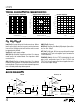
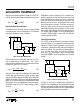
Quiescent Current vs Temperature Supply Current vs Switch Current Oscillator Frequency
SWITCH CURRENT (mA)
0
SUPPLY CURRENT (mA)
30
40
50
400 600 800
LT1173 •TPC07
1000
V = 5V
IN
20
10
0
V = 2V
IN
200
TEMPERATURE (°C)
–50
I ( A)
100
110
120
–25 0 25 50
LT1173 •TPC06
75
100
125
V = 3V
IN
IN
µ
90
V
IN
(V)
0
22.0
F
OSC
(kHz)
22.5
23.0
23.5
24.5
25.0
5101520
LT1173 • TPC08
24.0
25 30
25.5
26.0