
Datasheet


LT1173
5
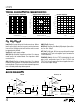
The LT1173 is a gated oscillator switcher. This type archi-
tecture has very low supply current because the switch is
cycled only when the feedback pin voltage drops below the
reference voltage. Circuit operation can best be under-
stood by referring to the LT1173 block diagram. Compara-
tor A1 compares the feedback pin voltage with the 1.245V
reference voltage. When feedback drops below 1.245V, A1
switches on the 24kHz oscillator. The driver amplifier
boosts the signal level to drive the output NPN power
switch. An adaptive base drive circuit senses switch
current and provides just enough base drive to ensure
switch saturation without overdriving the switch, resulting
in higher efficiency. The switch cycling action raises the
output voltage and feedback pin voltage. When the feed-
back voltage is sufficient to trip A1, the oscillator is gated
off. A small amount of hysteresis built into A1 ensures loop
stability without external frequency compensation. When
the comparator is low the oscillator and all high current
circuitry is turned off, lowering device quiescent current
to just 110µA, for the reference, A1 and A2.
The oscillator is set internally for 23µs ON time and 19µs
OFF time, optimizing the device for circuits where V
OUT
and V
IN
differ by roughly a factor of 2. Examples include a
3V to 5V step-up converter or a 9V to 5V step-down
converter.
U
LT1173 OPER
O
AT
I
A2 is a versatile gain block that can serve as a low battery
detector, a linear post regulator, or drive an under voltage
lockout circuit. The negative input of A2 is internally
connected to the 1.245V reference. A resistor divider from
V
IN
to GND, with the mid-point connected to the SET pin
provides the trip voltage in a low battery detector applica-
tion. The gain block output (AO) can sink 100µA (use a 47k
resistor pull-up to +5V). This line can signal a microcon-
troller that the battery voltage has dropped below the
preset level.
A resistor connected between the I
LIM
pin and V
IN
sets
maximum switch current. When the switch current ex-
ceeds the set value, the switch cycle is prematurely
terminated. If current limit is not used, I
LIM
should be tied
directly to V
IN
. Propagation delay through the current limit
circuitry is approximately 2µs.
In step-up mode the switch emitter (SW2) is connected to
ground and the switch collector (SW1) drives the induc-
tor; in step-down mode the collector is connected to V
IN
and the emitter drives the inductor.
The LT1173-5 and LT1173-12 are functionally identical to
the LT1173. The -5 and -12 versions have on-chip voltage
setting resistors for fixed 5V or 12V outputs. Pin 8 on the
fixed versions should be connected to the output. No
external resistors are needed.
U
S
A
O
PP
L
IC
AT
I
WU
U
I FOR ATIO
Measuring Input Current at Zero or Light Load
Obtaining meaningful numbers for quiescent current and
efficiency at low output current involves understanding
how the LT1173 operates. At very low or zero load current,
the device is idling for seconds at a time. When the output
voltage falls enough to trip the comparator, the power
switch comes on for a few cycles until the output voltage
rises sufficiently to overcome the comparator hysteresis.
When the power switch is on, inductor current builds up
to hundreds of milliamperes. Ordinary digital multimeters
are not capable of measuring average current because of
bandwidth and dynamic range limitations. A different
approach is required to measure the 100µA off-state and
500mA on-state currents of the circuit.
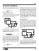
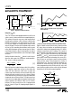
Quiescent current can be accurately measured using the
circuit in Figure 1. V
SET
is set to the input voltage of the
LT1173. The circuit must be “booted” by shorting V2 to
V
SET
. After the LT1173 output voltage has settled, discon-
nect the short. Input voltage is V2, and average input
current can be calculated by this formula:
I
VV
IN
=
−
()
21
100
01
Ω