
Datasheet


LT1173
9
keep V
FB
at the internal reference voltage of 1.245V. R1
and R2 set the output voltage according to the formula
V
R
R
V
OUT
=+
() ()
1
2
1
1 245 14..
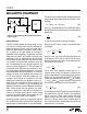
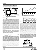
Step-Down (Buck Mode) Operation
A step-down DC-DC converter converts a higher voltage
to a lower voltage. The usual hookup for an LT1173 based
step-down converter is shown in Figure 6.
LT1173 • TA11
GND
SW2
SW1
LIM
I
IN
V
R3
100
FB
V
OUT
+
C2
+
C1
D1
1N5818
V
IN
R2
R1
L1
Ω
LT1173
Figure 6. Step-Down Mode Hookup
When the switch turns on, SW2 pulls up to V
IN
– V
SW
. This
puts a voltage across L1 equal to V
IN
– V
SW
– V
OUT
,
causing a current to build up in L1. At the end of the switch
ON time, the current in L1 is equal to
i
V
VV
L
t
PEAK
IN
SW OUT
ON
=
−−
()
.15
When the switch turns off, the SW2 pin falls rapidly and
actually goes below ground. D1 turns on when SW2
reaches 0.4V below ground.
D1 MUST BE A SCHOTTKY
DIODE
. The voltage at SW2 must never be allowed to go
below –0.5V. A silicon diode such as the 1N4933 will allow
SW2 to go to –0.8V, causing potentially destructive power
dissipation inside the LT1173. Output voltage is deter-
mined by
V
R
R
V
OUT
=+
() ()
1
2
1
1 245 16..
R3 programs switch current limit. This is especially im-
portant in applications where the input varies over a wide
range. Without R3, the switch stays on for a fixed time
each cycle. Under certain conditions the current in L1 can
build up to excessive levels, exceeding the switch rating
and/or saturating the inductor. The 100Ω resistor pro-
grams the switch to turn off when the current reaches
approximately 800mA. When using the LT1173 in step-
down mode, output voltage should be limited to 6.2V or
less. Higher output voltages can be accommodated by
inserting a 1N5818 diode in series with the SW2 pin
(anode connected to SW2).
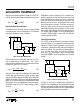
Inverting Configurations
The LT1173 can be configured as a positive-to-negative
converter (Figure 7), or a negative-to-positive converter
(Figure 8). In Figure 7, the arrangement is very similar to
a step-down, except that the high side of the feedback is
referred to ground. This level shifts the output negative.
As in the step-down mode, D1 must be a Schottky
diode, and V
OUT
should be less than 6.2V. More nega-
tive output voltages can be accomodated as in the prior
section.
Figure 7. Positive-to-Negative Converter
In Figure 8, the input is negative while the output is
positive. In this configuration, the magnitude of the input
voltage can be higher or lower than the output voltage. A
level shift, provided by the PNP transistor, supplies proper
polarity feedback information to the regulator.
U
S
A
O
PP
L
IC
AT
I
WU
U
I FOR ATIO
LT1173 • F07
–V
OUT
C2
+
C1
D1
1N5818
+V
IN
R1
R2
L1
GND
SW2
SW1
LIM
I
IN
V
R3
FB
LT1173
+