
Datasheet

2
LT1002
1002fb
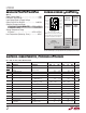
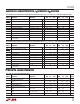
LT1002AM/LT1002AC LT1002M/LT1002C
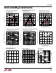
SYMBOL PARAMETER CONDITIONS MIN TYP MAX MIN TYP MAX UNITS
V
OS
Input Offset Voltage (Note 2) 20 60 25 100 µV
∆V
OS
Long Term Input Offset Voltage
∆Time
Stability (Notes 3 and 4) 0.3 1.5 0.4 2.0 µV/month
I
OS
Input Offset Current 0.3 2.8 0.4 4.2 nA
I
B
Input Bias Current ±0.6 ±3.0 ±0.7 ±4.5 nA
e
n
Input Noise Voltage 0.1Hz to 10Hz (Note 3) 0.35 0.7 0.38 0.75 µV
p-p
e
n
Input Noise Voltage Density f
O
= 10Hz (Note 6) 10.3 20.0 10.5 20.0
f
O
= 1000Hz (Note 3) 9.6 11.5 9.8 12.0 nV√Hz
A
VOL
Large Signal Voltage Gain R
L
≥ 2kΩ, V
O
= ±12V 400 800 350 800
V/mV
R
L
≥ 1kΩ, V
O
= ±10V 250 500 220 500
CMRR Common Mode Rejection Ratio V
CM
= ±13V 110 126 110 126 dB
PSRR Power Supply Rejection Ratio V
S
= ±3V to ±18V 108 123 105 123 dB
R
in
Input Resistance Differential Mode (Note 5) 20 100 13 80 MΩ
Input Voltage Range ±13 ±14 ±13 ±14 V
V
OUT
Maximum Output Voltage Swing R
L
≥ 2kΩ±13 ±14 ±13 ±14 V
R
L
≥ 1kΩ±12 ±13.5 ±12 ±13.5
SR Slew Rate R
L
≥ 2kΩ (Note 5) 0.1 0.25 0.1 0.25 V/µs
GBW Gain Bandwidth Product (Note 5) 0.4 0.8 0.4 0.8 MHz
P
d
Power Dissipation No load 46 75 48 85
mW
per amplifier No load, V
S
= ±3V 4 7 4 8
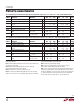
ABSOLUTE MAXIMUM RATINGS
W
WW
U
Supply Voltage (Note 7) ........................................ ±22V
Differential Input Voltage ...................................... ±30V
Input Voltage Equal to Supply Voltage
Output Short Circuit Duration ......................... Indefinite
Operating Temperature Range
LT1002AM/LT1002M (OBSOLETE) .. –55°C to 125°C
LT1002AC/LT1002C ............................... 0°C to 70°C
Storage Temperature Range
All Grades ......................................... –65°C to 150°C
Lead Temperature (Soldering, 10 sec.)................. 300°C
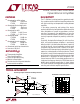
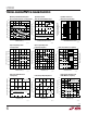
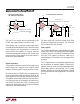
PACKAGE/ORDER INFORMATION
W
U
U
1
2
3
4
5
6
7
TOP VIEW
N PACKAGE
14 PIN PLASTIC
14
13
12
11
10
9
8
NULL (A)
NULL (A)
–IN (A)
+IN (A)
V– (B)
OUT (B)
V+ (B)
V+ (A)
OUT (A)
V– (A)
+IN (B)
–IN (B)
NULL (B)
NULL (B)
–
–
+
+
A
B
LT1002ACN
LT1002CN
OFFSET
VOLTAGE
MAX
at 25°C
ORDER
PART NO.
60µV
100µV
NOTE: Device may be operated even if insertion
is reversed; this is due to inherent symmetry of
pin locations of amplifiers A and B. (Note 7)
ELECTRICAL CHARACTERISTICS, I DIVIDUAL A PLIFIERS
UW
V
S
= ±15V, T
A
= 25°C, unless otherwise noted
Consult LTC Marketing for parts specified with wider operating temperature ranges.
(Note 1)
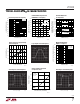
LT1002AMJ
LT1002MJ
LT1002ACJ
LT1002CJ
60µV
100µV
60µV
100µV
OBSOLETE PACKAGE
T
JMAX
= 125°C, θ
JA
= 100°C/W
J PACKAGE
14 PIN HERMETIC
T
JMAX
= 125°C, θ
JA
= 100°C/W
Consider the N Package for Alternate Source