
Datasheet

3
LT1002
1002fb
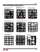
ELECTRICAL CHARACTERISTICS, I DIVIDUAL A PLIFIERS
UW
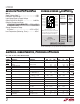
LT1002AM LT1002M
SYMBOL PARAMETER CONDITIONS MIN TYP MAX MIN TYP MAX UNITS
V
OS
Input Offset Voltage (Note 2) ● 30 150 45 230 µV
∆V
OS
Average Input Offset Voltage Drift ● 0.2 0.9 0.3 1.3 µV/°C
∆Temp
I
OS
Input Offset Current ● 0.8 5.6 1.2 8.5 nA
I
B
Input Bias Current ● ±1.0 ±6.0 ±1.5 ±9.0 nA
A
VOL
Large Signal Voltage Gain R
L
≥ 2kΩ, V
O
= ±10V ● 300 700 200 700 V/mV
CMRR Common Mode Rejection Ratio V
CM
= ±13V ● 106 122 104 120 dB
PSRR Power Supply Rejection Ratio V
S
= ±3V to ±18V ● 102 117 96 117 dB
Input Voltage Range ● ±13 ±14 ±13 ±14 V
V
OUT
Output Voltage Swing R
L
≥ 2kΩ ● ±12.5 ±13.5 ±12.0 ±13.5 V
P
d
Power Dissipation No load ● 55 90 60 100 mW
per amplifier
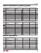
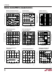
LT1002AC LT1002C
SYMBOL PARAMETER CONDITIONS MIN TYP MAX MIN TYP MAX UNITS
V
OS
Input Offset Voltage (Note 2) ● 20 100 30 160 µV
∆V
OS
Average Input Offset Voltage Drift ● 0.2 0.9 0.3 1.3 µV/°C
∆Temp
I
OS
Input Offset Current ● 0.5 4.2 0.6 5.7 nA
I
B
Input Bias Current ● ±0.7 ±4.5 ±1.0 ±6.0 nA
A
VOL
Large Signal Voltage Gain R
L
≥ 2kΩ, V
O
= ±10V ● 350 750 250 750 V/mV
CMRR Common Mode Rejection Ratio V
CM
= ±13V ● 108 124 106 123 dB
PSRR Power Supply Rejection Ratio V
S
= ±3V to ±18V ● 105 120 100 120 dB
Input Voltage Range ● ±13 ±14 ±13 ±14 V
V
OUT
Output Voltage Swing R
L
≥ 2kΩ ● ±12.5 ±13.8 ±12.5 ±13.8 V
P
d
Power Dissipation No Load ● 50 85 55 90 mW
per amplifier
The ● denotes the specifications which apply over the temperature range –55°C ≤ T
A
≤ 125°C, V
S
= ±15V,unless otherwise noted.
The ● denotes the specifications which apply over the temperature range 0°C ≤ T
A
≤ 70°C, V
S
= ±15V, unless otherwise noted.
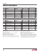
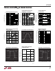
LT1002AM/AC LT1002M/C
SYMBOL PARAMETER CONDITIONS MIN TYP MAX MIN TYP MAX UNITS
Input Offset Voltage Match – 15 40 – 25 80 µV
I
B
+
Average Non-Inverting Bias
Current – ±0.6 ±3.5 – ±0.7 ±4.8 nA
I
OS
+
Non-Inverting Offset Current – 0.6 3.5 – 0.7 6.0 nA
I
OS
–
Inverting Offset Current – 0.6 3.5 – 0.7 6.0 nA
∆CMRR Common Mode Rejection Ratio
Match V
CM
= ±13V 110 132 – 108 132 – dB
∆PSRR Power Supply Rejection Ratio
Match V
S
= ±3V to ±18V 108 130 – 102 128 – dB
Channel Seperation f ≤ 10Hz (Note 5) 132 148 – 130 146 – dB
ATCHI G CHARACTERISTICS
UW
V
S
= ±15V, T
A
= 25°C, unless otherwise noted.