
Datasheet

4
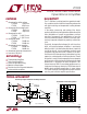
LT1002
1002fb
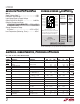
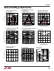
The ● denotes the specifications which apply over the temperature range 0°C ≤ T
A
≤ 70°C, V
S
= ±15V, unless otherwise noted.
LT1002AM LT1002M
SYMBOL PARAMETER CONDITIONS MIN TYP MAX MIN TYP MAX UNITS
Input Offset Voltage Match ● – 50 140 – 60 230 µV
Input Offset Voltage Tracking ● – 0.3 1.0 – 0.4 1.5 µV/°C
I
B
+
Average Non-Inverting Bias
Current ● – ±1.5 ±6.0 – ±1.8 ±10.0 nA
I
OS
+
Non-Inverting Offset Current ● – 1.5 6.5 – 1.8 12.0 nA
I
OS
–
Inverting Offset Current ● – 1.5 6.5 – 1.8 12.0 nA
∆CMRR Common Mode Rejection Ratio
Match V
CM
= ±13V ● 106 126 102 124 – dB
∆PSRR Power Supply Rejection Ratio
Match V
S
= ±3V to ±18V ● 102 122 94 120 – dB
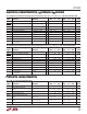
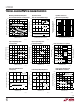
ATCHI G CHARACTERISTICS
UW
LT1002AC LT1002C
SYMBOL PARAMETER CONDITIONS MIN TYP MAX MIN TYP MAX UNITS
Input Offset Voltage Match ● – 30 85 – 45 150 µV
Input Offset Voltage Tracking ● – 0.3 1.0 – 0.4 1.5 µV/°C
I
B
+
Average Non-Inverting Bias
Current ● – ±1.0 ±4.5 – ±1.2 ±7.0 nA
I
OS
+
Non-Inverting Offset Current ● – 1.0 5.0 – 1.2 8.5 nA
I
OS
–
Inverting Offset Current ● – 1.0 5.0 – 1.2 8.5 nA
∆CMRR Common Mode Rejection Ratio
Match V
CM
= ±13V ● 108 130 – 105 128 – dB
∆PSRR Power Supply Rejection Ratio
Match V
S
= ±3V to ±18V ● 105 126 – 98 124 – dB
For MIL-STD components, please refer to LTC 883C data sheet for test
listing and parameters.
Note 1: Absolute Maximum Ratings are those values beyond which the life
of a device may be impaired.
Note 2: Offset voltage measured with high speed test equipment,
approximately 1second after power is applied.
Note 3: This parameter is tested on a sample basis only.
Note 4: Long Term Input Offset Voltage Stability refers to the averaged
trend line of V
OS
versus Time over extended periods after the first 30 days
of operation. Excluding the initial hour of operation, changes in V
OS
during
the first 30 operating days are typically 2.5µV.
Note 5: Parameter is guaranteed by design.
Note 6: 10Hz noise voltage density is sample tested on every lot.
Devices 100% tested at 10Hz are available on request.
Note 7: The V+ supply terminals are completely independent and may be
powered by separate supplies if desired (this approach, however, would
sacrifice the advantages of the power supply rejection ratio matching). The
V– supply terminals are both connected to the common substrate and
must be tied to the same voltage. Both V– pins should be used.
The ● denotes the specifications which apply over the temperature range –55°C ≤ T
A
≤ 125°C, V
S
= ±15V, unless otherwise noted.