
Datasheet


LT1010
10
1010fe
APPLICATIONS INFORMATION
This is a good example of how fast op amps can be made
quite easy to use by employing an output buffer.
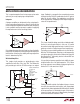
Integrator
A lowpass amplifier can be formed just by using large C
F
in the inverter described earlier, as long as the increasing
closed-loop output impedance above the cutoff frequency
is not a problem and the op amp is capable of supplying
the required current at the summing junction.
stage. Feedback is arranged in the conventional manner,
although the 68µF-0.01µF combination limits DC gain to
unity for all gain settings. For applications sensitive to
NTSC requirements, dropping the 25Ω output stage bias
value will aid performance.
A2
LT1010
R
F
20k
C
F
500pF
C
I
I
IN
1010 AI07
V
OUT
–
+
A1
LT1012
If the integrating capacitor must be driven from the buffer
output, the circuit above can be used to provide capacitive
load isolation. As before, the stability with large capacitive
loads is determined by R
F
C
F
.
Wideband Amplifiers
This simple circuit provides an adjustable gain video
amplifier that will drive 1V
P-P
into 75Ω. The differential
pair provides gain with the LT1010 serving as an output
BIAS
+
LT1010
22µF
+
22µF
TYPICAL SPECIFICATIONS
1V
P-P
INTO 75Ω
AT A = 2
0.5dB TO 10MHz
3dB DOWN AT 16MHz
AT A = 10
0.5dB TO 4MHz
–3dB = 8MHz
+
68µF
1010 AI08
PEAKING
5pF to 25pF
25Ω
900Ω
OUTPUT
(75Ω)
0.01µF
1k
GAIN SET
5.1k
Q1, Q2: 2N3866
–15V
8.2k
15V
–15V
Q2Q1INPUT
A2
LT1010
R1
100Ω
R2
800Ω
C1
15pF
V
IN
1010 AI09
V
OUT
–
+
A1
HA2625
This shows the buffer being used with a wideband ampli-
fier that is not unity-gain stable. In this case, C1 cannot
be used to isolate large capacitive loads. Instead, it has an
optimum value for a limited range of load capacitances.
The buffer can cause stability problems in circuits like this.
With the TO-220 packages, behavior can be improved by
raising the quiescent current with a 20Ω resistor from the
bias terminal to V
+
. Alternately, devices in the miniDIP can
be operated in parallel.
It is possible to improve capacitive load stability by oper-
ating the buffer class A at high frequencies. This is done
by using quiescent current boost and bypassing the bias
terminal to V
–
with more than 0.02µF.
A2
LT1010
R1
400Ω
R2
1.6k
INPUT
1010 AI10
OUTPUT
–
+
A1
HA2625
Putting the buffer outside the feedback loop as shown
here will give capacitive load isolation, with large output
capacitors only reducing bandwidth. Buffer offset, referred
to the op amp input, is divided by the gain. If the load re-
sistance is known, gain error is determined by the output
resistance tolerance. Distortion is low.