
Datasheet

6
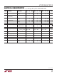
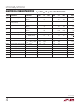
LT1012A/LT1012
sn1012 1012afbs
LT1012AC LT1012C
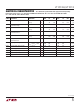
SYMBOL PARAMETER CONDITIONS MIN TYP MAX MIN TYP MAX UNITS
V
OS
Input Offset Voltage ● 20 60 20 100 µV
(Note 3)
● 30 160 30 200 µV
Average Temperature Coefficient of ● 0.2 0.6 0.2 1.0 µV/°C
Input Offset Voltage
I
OS
Input Offset Current ● 25 230 35 230 pA
(Note 3)
● 40 300 45 300 pA
Average Temperature Coefficient of ● 0.3 2.5 0.3 2.5 pA/°C
Input Offset Current
I
B
Input Bias Current ● ± 35 ± 230 ± 35 ± 230 pA
(Note 3)
● ± 50 ± 300 ± 50 ± 300 pA
Average Temperature Coefficient of ● 0.3 2.5 0.3 2.5 pA/°C
Input Bias Current
A
VOL
Large-Signal Voltage Gain V
OUT
= ±12V, R
L
≥ 10kΩ ● 200 1500 150 1500 V/mV
V
OUT
= ±10V, R
L
≥ 2kΩ ● 200 1000 150 800 V/mV
CMRR Common Mode Rejection Ratio V
CM
= 13.5V ● 110 130 108 130 dB
PSRR Power Supply Rejection Ratio V
S
= ±1.3V to ± 20V ● 110 128 108 128 dB
Input Voltage Range ● ±13.5 ±13.5 V
V
OUT
Output Voltage Swing R
L
= 10kΩ ● ±13 ±14 ±13 ±14 V
I
S
Supply Current ● 400 600 400 800 µA
The ● denotes the specifications which apply over the full operating
temperature range of 0°C ≤ T
A
≤ 70°C. V
S
= ± 15V, V
CM
= 0V, unless otherwise noted.
ELECTRICAL CHARACTERISTICS