
Datasheet


5
LT1013/LT1014
10134fb
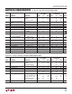
The ● denotes the specifications which apply over the temperature range
–40°C ≤ T
A
≤ 85°C for LT1013I, LT1014I, 0°C ≤ T
A
≤ 70°C for LT1013C, LT1013D, LT1014C, LT1014D. V
S
= ±15V, V
CM
= 0V unless
otherwise noted.
LT1013C/D/I
LT1013AC LT1014AC LT1014C/D/I
SYMBOL PARAMETER CONDITIONS MIN TYP MAX MIN TYP MAX MIN TYP MAX UNITS
V
OS
Input Offset Voltage ● — 55 240 — 65 270 — 80 400 µV
LT1013D/I, LT1014D/I
● — — — — — — — 230 1000 µV
V
S
= +5V, 0V; V
O
= 1.4V ● — 75 350 — 85 380 — 110 570 µV
LT1013D/I, LT1014D/I
V
S
= +5V, 0V; V
O
= 1.4V ● — — — — — — — 280 1200 µV
Average Input Offset (Note 3)
● — 0.3 2.0 — 0.3 2.0 — 0.4 2.5 µV/°C
Voltage Drift LT1013D/I, LT1014D/I ● ———————0.75.0µV/°C
I
OS
Input Offset Current ● — 0.2 1.5 — 0.2 1.7 — 0.3 2.8 nA
V
S
= +5V, 0V; V
O
= 1.4V ● — 0.4 3.5 — 0.4 4.0 — 0.5 6.0 nA
I
B
Input Bias Current ● — 13 25 — 13 25 — 16 38 nA
V
S
= +5V, 0V; V
O
= 1.4V ● — 18 55 — 20 60 — 24 90 nA
A
VOL
Large Signal Voltage Gain V
O
= ±10V, R
L
= 2k ● 1.0 5.0 — 1.0 5.0 — 0.7 4.0 — V/µV
CMRR Common Mode Rejection V
CM
= +13.0V, –15.0V ● 98 116 — 98 116 — 94 113 — dB
Ratio
PSRR Power Supply Rejection V
S
= ±2V to ±18V ● 101 119 — 101 119 — 97 116 — dB
Ratio
V
OUT
Output Voltage Swing R
L
= 2k ● ±12.5 ±13.9 — ±12.5 ±13.9 — ±12.0 ±13.9 — V
V
S
= +5V, 0V; R
L
= 600Ω
Output Low
● — 613— 613— 613 mV
Output High ● 3.3 3.9 — 3.3 3.9 — 3.2 3.9 — V
I
S
Supply Current per Amplifier ● — 0.36 0.55 — 0.36 0.55 — 0.37 0.60 mA
V
S
= +5V, 0V; V
O
= 1.4V ● — 0.32 0.50 — 0.32 0.50 — 0.34 0.55 mA
ELECTRICAL CHARACTERISTICS
Note 1: Absolute Maximum Ratings are those values beyond which the life
of a device may be impaired.
Note 2: This parameter is guaranteed by design and is not tested. Typical
parameters are defined as the 60% yield of parameter distributions of
individual amplifiers; i.e., out of 100 LT1014s (or 100 LT1013s) typically
240 op amps (or 120 ) will be better than the indicated specification.
Note 3: This parameter is not 100% tested.