
Datasheet
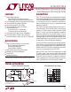


LT1013/LT1014
6
10134fd
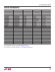
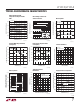
elecTrical characTerisTics
SYMBOL PARAMETER CONDITIONS
LT1013AC LT1014AC
LT1013C/D/I
LT1014C/D/I
UNITSMIN TYP MAX MIN TYP MAX MIN TYP MAX
V
OS
Input Offset Voltage
LT1013D/I, LT1014D/I
V
S
= 5V, 0V; V
O
= 1.4V
LT1013D/I, LT1014D/I
V
S
= 5V, 0V; V
O
= 1.4V
l
l
l
l
55
75
240
350
65
85
270
380
80
230
110
280
400
1000
570
1200
µV
µV
µV
µV
Average Input Offset
Voltage Drift
(Note 3)
LT1013D/I, LT1014D/I
l
l
0.3 2.0 0.3 2.0 0.4
0.7
2.5
5.0
µV/°C
µV/°C
I
OS
Input Offset Current
V
S
= 5V, 0V; V
O
= 1.4V
l
l
0.2
0.4
1.5
3.5
0.2
0.4
1.7
4.0
0.3
0.5
2.8
6.0
nA
nA
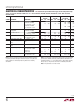
I
B
Input Bias Current
V
S
= 5V, 0V; V
O
= 1.4V
l
l
13
18
25
55
13
20
25
60
16
24
38
90
nA
nA
A
VOL
Large-Signal Voltage Gain V
O
= ±10V, R
L
= 2k
l
1.0 5.0 1.0 5.0 0.7 4.0 V/µV
CMRR Common Mode Rejection
Ratio
V
CM
= 13.0V, –15.0V
l
98 116 98 116 94 113 dB
PSRR Power Supply Rejection
Ratio
V
S
= ±2V to ±18V
l
101 119 101 119 97 116 dB
V
OUT
Output Voltage Swing R
L
= 2k
V
S
= 5V, 0V; R
L
= 600Ω
Output Low
Output High
l
l
l
±12.5
3.3
±13.9
6
3.9
13
±12.5
3.3
±13.9
6
3.9
13
±12.0
3.2
±13.9
6
3.9
13
V
mV
V
I
S
Supply Current per Amplifier
V
S
= 5V, 0V; V
O
= 1.4V
l
l
0.36
0.32
0.55
0.50
0.36
0.32
0.55
0.50
0.37
0.34
0.60
0.55
mA
mA
Note 1: Stresses beyond those listed under Absolute Maximum Ratings
may cause permanent damage to the device. Exposure to any Absolute
Rating condition for extended periods may affect device reliability
and lifetime.
The l denotes the specifications which apply over the temperature range
–40°C ≤ T
A
≤ 85°C for LT1013I, LT1014I, 0°C ≤ T
A
≤ 70°C for LT1013C, LT1013D, LT1014C, LT1014D. V
S
= ±15V, V
CM
= 0V unless
otherwise noted.
Note 2: This parameter is guaranteed by design and is not tested. Typical
parameters are defined as the 60% yield of parameter distributions of
individual amplifiers; i.e., out of 100 LT1014s (or 100 LT1013s) typically
240 op amps (or 120 ) will be better than the indicated specification.
Note 3: This parameter is not 100% tested.