
Datasheet


LT1016
15
1016fc
Typical applicaTions
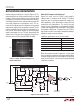
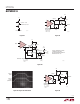
1MHz to 10MHz Crystal
Oscillator
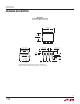
18ns Fuse with Voltage Programmable Trip Point
–
+
LT1016
0.068µF
2k
GND
LATCH
V
–
1MHz TO 10MHz
CRYSTAL
2k
2k
5V
5V
V
+
Q
Q
1016 AI04
OUTPUT
–
+
A2
LT1016
–
+
A1
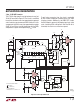
LT1193
RESET (NORMALLY OPEN)
900Ω
200Ω
CALIBRATE
FB
1k*
1k*
9k*
9k*
LOAD
10Ω
CARBON
TRIP SET
0mA TO 250mA = 0V TO 2.5V
28V
Q1
2N3866
Q2
2N2369
330Ω
2.4k
–5V
33pF
300Ω
1k
* = 1% FILM RESISTOR
A1 AND A2 USE 5V SUPPLIES
L
1016 AI05
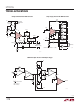
appenDix a
About Level Shifts
The TTL output of the LT1016 will interface with many
circuits directly. Many applications, however, require some
form of level shifting of the output swing. With LT1016
based circuits this is not trivial because it is desirable to
maintain very low delay in the level shifting stage. When
designing level shifters, keep in mind that the TTL output of
the LT1016 is a sink-source pair (Figure A1) with good abil
-
ity to
drive capacitance (such as feedforward capacitors).
Figure
A2 shows a noninverting voltage gain stage with a
15V output. When the LT1016 switches, the base-emitter
voltages at the 2N2369 reverse, causing it to switch very
quickly. The 2N3866 emitter-follower gives a low imped
-
ance output
and the Schottky diode aids current sink
capability.
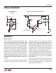
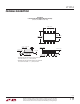
Figure
A3 is a very versatile stage. It features a bipolar
swing that may be programmed by varying the output
transistor’s supplies. This 3ns delay stage is ideal for
driving FET switch gates. Q1, a gated current source,
switches the Baker-clamped output transistor, Q2. The
heavy feedforward capacitor from the LT1016 is the key
to low delay, providing Q2’s base with nearly ideal
drive.
This
capacitor loads the LT1016’s output transition (Trace
A, Figure A4), but Q2’s switching is clean (Trace B, Figure
A4) with 3ns delay on the rise and fall of the pulse.
Figure A5 is similar to Figure A2 except that a sink transistor
has replaced the Schottky diode. The two emitter-followers
drive a power MOSFET which switches 1A at 15V. Most of
the 7ns to 9ns delay in this stage occurs in the MOSFET
and the 2N2369.
When designing level shifters, remember to use transistors
with fast switching times and high f
T
s. To get the kind of
results shown, switching times in the ns range and f
T
s
approaching 1GHz are required.