
Datasheet

7
LT1019
1019fd
the thermal regulation specification. Example: a 10V
device with a nominal input voltage of 15V and load
current of 5mA. Find the effect of an input voltage change
of 1V and a load current change of 2mA.
∆P (line change) = (∆V
IN
)(I
LOAD
) = (1V)(5mA) = 5mW
∆V
OUT
= (0.5ppm/mW)(5mW) = 2.5ppm
∆P (load change) = (∆I
LOAD
)(V
IN
– V
OUT
)
= (2mA)(5V) = 10mW
∆V
OUT
= (0.5ppm/mW)(10mW) = 5ppm
Even though these effects are small, they should be taken
into account in critical applications, especially where input
voltage or load current is high.
The second thermal effect is overall die temperature
change. The magnitude of this change is the product of
change in power dissipation times the thermal resistance
(θ
JA
) of the IC package ≅ (100°C/W to 150°C/W). The
effect on the reference output is calculated by multiplying
die temperature change by the temperature drift specifica-
tion of the reference. Example: same conditions as above
with θ
JA
= 150°C/W and an LT1019 with 20ppm/°C drift
specification.
∆P (line change) = 5mW
∆V
OUT
= (5mW)(150°C/W)(20ppm/°C)
= 15ppm
∆P (load change) = 10mW
∆V
OUT
= (10mW)(150°C/W)(20ppm/°C)
= 30ppm
These calculations show that thermally induced output
voltage variations can easily exceed the electrical effects.
In critical applications where shifts in power dissipation
are expected, a small clip-on heat sink can significantly
improve these effects by reducing overall die temperature
change. Alternately, an LT1019A can be used with four
times lower TC. If warm-up drift is of concern, these
measures will also help. With warm-up drift,
total
device
power dissipation must be considered. In the example
given, warm-up drift (worst case) is equal to:
Warm-up drift = [(V
IN
)(I
Q
) + (V
IN
– V
OUT
)(I
LOAD
)]
[(θ
JA
)(TC)]
with I
Q
(quiescent current) = 0.6mA,
Warm-up drift = [(15V)(0.6mA) + (5V)(5mA)]
[(150°C/W)(25ppm/°C)]
= 127.5ppm
Note that 74% of the warm-up drift is due to load current
times input/output differential. This emphasizes the
importance of keeping both these numbers low in critical
applications.
Note that line regulation is now affected by reference
output impedance. R1 should have a wattage rating high
enough to withstand full input voltage if output shorts
must be tolerated. Even with load currents below 10mA,
R1 can be used to reduce power dissipation in the LT1019
for lower warm-up drift, etc.
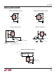
Output Trimming
Output voltage trimming on the LT1019 is nominally
accomplished with a potentiometer connected from out-
put to ground with the wiper tied to the trim pin. The
LT1019 was made compatible with existing references, so
the trim range is large: +6%, – 6% for the LT1019-2.5,
+5%, – 13% for the LT1019-5, and +5%, –27% for the
LT1019-10. This large trim range makes precision trim-
ming rather difficult. One solution is to insert resistors in
series with both ends of the potentiometer. This has the
disadvantage of potentially poor tracking between the
fixed resistors and the potentiometer. A second method of
reducing trim range is to insert a resistor in series with the
wiper of the potentiometer. This works well only for very
small trim range because of the mismatch in TCs between
the series resistor and the internal thin film resistors.
These film resistors can have a TC as high as 500ppm/°C.
That same TC is then transferred to the change in output
voltage: a 1% shift in output voltage causes a
(500ppm)(1%) = 5ppm/°C change in output voltage drift.
APPLICATIO S I FOR ATIO
UU W U