
Datasheet

8
LT1019
1019fd
The worst-case error in initial output voltage for the
LT1019 is 0.2%, so a series resistor is satisfactory if the
output is simply trimmed to nominal value. The maximum
TC shift expected would be 1ppm/°C.
Using the Temp Pin
The LT1019 has a TEMP pin like several other bandgap
references. The voltage on this pin is directly propor-
tional to absolute temperature (PTAT) with a slope of
approximately 2.1mV/°C. Room temperature voltage is
therefore approximately (295°K)(2.1mV/°C) = 620mV.
This voltage varies with process parameters and should
not be used to measure absolute temperature, but
rather relative temperature changes. Previous bandgap
references have been very sensitive to any loading on
the TEMP pin because it is an integral part of the
reference “core” itself. The LT1019 “taps” the core at a
special point which has much less effect on the refer-
ence. The relationship between TEMP pin loading and
a change in reference output voltage is less than
0.05%/µA, about ten times improvement over previous
references.
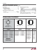
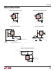
Output Bypassing
The LT1019 is designed to be stable with a wide range of
load currents and output capacitors. The 4.5V, 5V, and
10V devices do not oscillate under any combination of
capacitance and load. The 2.5V device can oscillate when
sinking currents between 1mA and 6mA for load capaci-
tance between 400pF and 2µF (see Figure 1).
If output bypassing is desired to reduce high frequency
output impedance, keep in mind that loop phase margin is
significantly reduced for output capacitors between 500pF
and 1µF if the capacitor has low ESR (Effective Series
Resistance). This can make the output “ring” with tran-
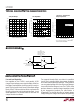
Figure 1. Output Bypassing
sient loads. The best transient load response is obtained
by deliberately adding a resistor to increase ESR as shown
in Figure 1.
Use configuration (a) if DC voltage error cannot be com-
promised as load current changes. Use (b) if absolute
minimum peak perturbation at the load is needed. For best
transient response, the output can be loaded with ≥ 1mA
DC current.
APPLICATIO S I FOR ATIO
UU W U
TYPICAL APPLICATIO S
U
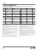
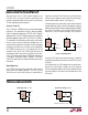
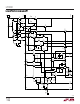
Wide Range Trim ≥ ±5%
Narrow Trim Range (±0.2%)
V
IN
2Ω TO 5Ω
LT1019
1019 F01
2µF
TANTALUM
V
IN
LT1019
2µF TO 10µF
TANTALUM
2Ω TO 5Ω
(a) (b)
+
+
V
OUT
R1
25k
OUT
IN
LT1019
TRIM
GND
V
IN
1019 TA03
V
OUT
R1
100k
OUT
IN
LT1019
TRIM
GND
V
IN
1019 TA05
R2*
1.5M
*INCREASE TO 4.7M FOR LT1019A (±0.05%)