
Datasheet


6
LT1019
1019fd
CCHARA TERIST
ICS
UW
AT
Y
P
I
CA
LPER
F
O
R
C
E
JUNCTION TEMPERATURE (°C)
–50
0.40
VOLTAGE (V)
0.45
0.55
0.60
0.65
0.90
0.75
0
50
75
LT1019 • TPC10
0.50
0.80
0.85
0.70
–25
25
100
125
Temp Pin Voltage
INPUT VOLTAGE (V)
0
–30
OUTPUT VOLTAGE CHANGE (µV)
–20
0
20
40
140
80
10
20
25
LT1019 • TPC11
–10
100
120
60
515
30
35
40
LT1019-2.5
LT1019-5
I
OUT
T
J
= 25°C
LT1019-10
Line Regulation
LT1019-2.5* Stability with
Output Capacitance
*LT1019-4.5/LT1019-5/LT1019-10 ARE STABLE
WITH ALL LOAD CAPACITANCE.
OUTPUT CURRENT (mA)
0.01
OUTPUT CAPACITOR (µF)
0.1
20 0 10
1019 G12
0.001
10
20
0.0001
1
10
15 5 5 15
SINK CURRENT SOURCE CURRENT
REGION OF POSSIBLE
INSTABILITY
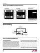
–
+
V
IN
1.188V
V
OUT
GND
R2
LT1019-4.5, LT1019-5,
LT1019-10 = 5k
LT1019-2.5 = 10k
R3
80k
TRIM
LT1019-2.5 = 11k
LT1019-4.5 = 13.9k
LT1019-5 = 16k
LT1019-10 = 37.1k
R1
LT1019 • BD
BLOCK DIAGRA
W
APPLICATIO S I FOR ATIO
UU W U
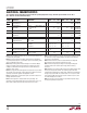
Line and Load Regulation
Line regulation on the LT1019 is nearly perfect. A 10V
change in input voltage causes a typical output shift of less
than 5ppm. Load regulation (sourcing current) is nearly as
good. A 5mA change in load current shifts output voltage
by only 100µV. These are
electrical
effects, measured with
low duty cycle pulses to eliminate heating effects. In real
world applications, the
thermal
effects of load and line
changes must be considered.
Two separate thermal effects are evident in monolithic
circuits. One is a gradient effect, where power dissipation
on the die creates temperature gradients. These gradients
can cause output voltage shifts
even if the overall tempera-
ture coefficient of the reference is zero
. The LT1019, unlike
previous references, specifies thermal regulation caused
by die temperature gradients.The specification is
0.5ppm/mW. To calculate the effect on output voltage,
simply multiply the
change
in device power dissipation by