
Datasheet

10
LT1021
APPLICATIONS INFORMATION
WUU
U
minimized. In the current output circuit, R1 determines
output current. It should have a TC commensurate with the
LT1021 or track closely with the feedback resistor around
the op amp.
Kelvin Connections
Although the LT1021 does not have true force/sense
capability at its outputs, significant improvements in ground
loop and line loss problems can be achieved with proper
hook-up. In series mode operation, the ground pin of the
LT1021 carries only ≈1mA and can be used as a sense
line, greatly reducing ground loop and loss problems on
the low side of the reference. The high side supplies load
current so line resistance must be kept low. Twelve feet of
#22 gauge hook-up wire or 1 foot of 0.025 inch printed
circuit trace will create 2mV loss at 10mA output current.
This is equivalent to 1LSB in a 10V, 12-bit system.
The following circuits show proper hook-up to minimize
errors due to ground loops and line losses. Losses in the
output lead can be greatly reduced by adding a PNP boost
transistor if load currents are 5mA or higher. R2 can be
added to further reduce current in the output sense lead.
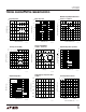
Capacitive Loading and Transient Response
The LT1021 is stable with all capacitive loads, but for
optimum settling with load transients, output capacitance
should be under 1000pF. The output stage of the reference
is class AB with a fairly low idling current. This makes
transient response worst-case at light load currents. Be-
cause of internal current drain on the output, actual worst-
case occurs at I
LOAD
= 0 on LT1021-5, I
LOAD
=
–0.8mA (sinking) on LT1021-7 and I
LOAD
= 1.4mA (sink-
ing) on LT1021-10. Significantly better load transient
response is obtained by moving slightly away from these
points. See Load Transient Response curves for details. In
general, best transient response is obtained when the
output is sourcing current. In critical applications, a 10µF
solid tantalum capacitor with several ohms in series
provides optimum output bypass.
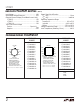
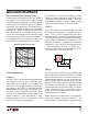
Standard Series Mode
LT1021
OUT
IN
GND
KEEP THIS LINE RESISTANCE LOW
LOAD
+
INPUT
GROUND
RETURN
1021 AI05
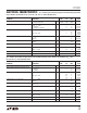
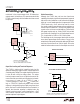
Series Mode with Boost Transistor
LT1021-7
OUT
IN
GND
R3
50k
RESISTOR TC DETERMINES I
OUT
TC
TC ≤ (10 • R1) TC. R2 AND R3 SCALE
WITH R1 FOR DIFFERENT OUTPUT CURRENTS
*
**
R1*
7.15k
1.000mA
R2**
182k
1021 AI04
–
+
OP AMP
LT1021-7
OUT
IN
TC TRACKING TO 50ppm/°C
GND
R3
10k
R1*
200Ω
1%
V
OUT
6.950V
R2*
14k
1%
1021 AI03
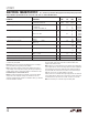
LT1021
OUT
GND
IN
LOAD
R1
220Ω
2N3906
R2*
INPUT
GROUND
RETURN
*OPTIONAL—REDUCES CURRENT IN OUTPUT SENSE LEAD
R2 = 2.4k (LT1021-5), 3k (LT1021-7), 5.6k (LT1021-10)
1021 AI06