
Datasheet

9
LT1021
APPLICATIONS INFORMATION
WUU
U
Maximum Allowable Reference Drift
Trimming Output Voltage
LT1021-10
The LT1021-10 has a trim pin for adjusting output voltage.
The impedance of the trim pin is about 12kΩ with a
nominal open-circuit voltage of 5V. It is designed to be
driven from a source impedance of 3kΩ or less to mini-
mize changes in the LT1021 TC with output trimming.
Attenuation between the trim pin and the output is 70:1.
This allows ±70mV trim range when the trim pin is tied to
the wiper of a potentiometer connected between the
output and ground. A 10kΩ potentiometer is recom-
mended, preferably a 20 turn cermet type with stable
characteristics over time and temperature.
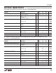
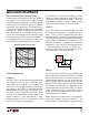
Effect of Reference Drift on System Accuracy
A large portion of the temperature drift error budget in
many systems is the system reference voltage. This graph
indicates the maximum temperature coefficient allowable
if the reference is to contribute no more than 0.5LSB error
to the overall system performance. The example shown is
a 12-bit system designed to operate over a temperature
range from 25°C to 65°C. Assuming the system calibra-
tion is performed at 25°C, the temperature span is 40°C.
It can be seen from the graph that the temperature coeffi-
cient of the reference must be no worse than 3ppm/°C if
it is to contribute less than 0.5LSB error. For this reason,
the LT1021 family has been optimized for low drift.
The LT1021-10 “C” version is pre-trimmed to ±5mV and
therefore can utilize a restricted trim range. A 75k resistor
in series with a 20kΩ potentiometer will give ±10mV trim
range. Effect on the output TC will be only 1ppm/°C for the
±5mV trim needed to set the “C” device to 10.000V.
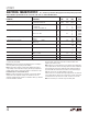
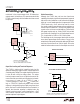
LT1021-5
The LT1021-5 does have an output voltage trim pin, but
the TC of the nominal 4V open-circuit voltage at this pin is
about –1.7mV/°C. For the voltage trimming not to affect
reference output TC, the external trim voltage must track
the voltage on the trim pin. Input impedance of the trim pin
is about 100kΩ and attenuation to the output is 13:1. The
technique shown below is suggested for trimming the
output of the LT1021-5 while maintaining minimum shift
in output temperature coefficient. The R1/R2 ratio is
chosen to minimize interaction of trimming and TC shifts,
so the exact values shown should be used.
LT1021-5
OUT
IN
GND
TRIM
R1
27k
R2
50k
1N4148
V
OUT
1021 AI02
TEMPERATURE SPAN (°C)
100
MAXIMUM TEMPERATURE COEFFICIENT FOR
0.5LSB ERROR (ppm/°C)
30
100
LT1021 AI01
1.0
10
20 100
90
807060
50
40
8-BIT
10-BIT
12-BIT
14-BIT
LT1021-7
The 7V version of the LT1021 has no trim pin because the
internal architecture does not have a point which could be
driven conveniently from the output. Trimming must
therefore be done externally, as is the case with ordinary
reference diodes. Unlike these diodes, however, the out-
put of the LT1021 can be loaded with a trim potentiometer.
The following trim techniques are suggested; one for
voltage output and one for current output. The voltage
output is trimmed for 6.95V. Current output is 1mA, as
shown, into a summing junction, but all resistors may be
scaled for currents up to 10mA.
Both of these circuits use the trimmers in a true potentio-
metric mode to reduce the effects of trimmer TC. The
voltage output has a 200Ω impedance, so loading must be