
Datasheet

3
LT1039/LT1039-16
1039fd
ELECTRICAL CHARACTERISTICS
PARAMETER CONDITIONS MIN TYP MAX UNITS
Receiver V
CC
= 5V, V
ON/OFF
= 2.5V (Note 2)
Input Voltage Thresholds Input Low Level (V
OUT
= High) ● 0.5 1.3 V
Input High Level (V
OUT
= Low) ● 1.7 2.8 V
Hysteresis ● 0.1 0.4 1.0 V
Input Resistance ● 30 kΩ
Output Voltage Output Low, I
OUT
= –1.6mA ● 0.4 0.5 V
Output High, I
OUT
= 160µA ● 3.5 4.8 V
Output Short-Circuit Current Sourcing Current, V
OUT
= 0V (Note 5) ● 0.5 1 mA
Sinking Current, V
OUT
= V
CC
● –10 mA
Output Leakage Current Shutdown (Note 2), 0V ≤ V
OUT
≤ V
CC
, V
IN
= 0V ● 110µA
Supply Current ● 47mA
Supply Leakage Current Shutdown (Note 3) ● 1 (25°C) 100 µA
ON/OFF Pin Current 0V ≤ V
ON/OFF
≤ 5V ● –15 80 µA
Note 1: Absolute Maximum Ratings are those values beyond which the life
of a device by be impaired.
Note 2: V
ON/OFF
= 5V for LT1039M grade devices.
Note 3: V
ON/OFF
= 0.4V for –55°C ≤ T
A
≤ 100°C and V
ON/OFF
= 0.2V for
100°C ≤ T
A
≤ 125°C. Does not apply to LT1039-16 part.
Note 4: For T
A
≥ 100°C, leakage current is 350µA max.
Note 5: For T
A
≤ –25°C, output source current is 0.4mA.
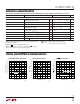
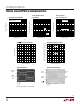
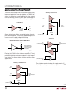
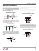
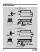
TYPICAL PERFORMANCE CHARACTERISTICS
U
W
Driver Output Short-Circuit Current ON/OFF Pin ThresholdsReceiver Input Thresholds
TEMPERATURE (°C)
–55
0
OUTPUT CURRENT (mA)
5
15
20
25
50
35
0
50
75
1039 G01
10
40
45
30
–25
25
100
125
SINKING
SOURCING
TEMPERATURE (°C)
–55
0.50
INPUT VOLTAGE (V)
0.75
1.25
1.50
1.75
3.00
2.25
0
50
75
1039 G02
1.00
2.50
2.75
2.00
–25
25
100
125
INPUT HIGH
INPUT LOW
TEMPERATURE (°C)
–55
0
ON/OFF PIN VOLTAGE (V)
0.5
1.5
2.0
2.5
5.0
3.5
0
50
75
1039 G03
1.0
4.0
4.5
3.0
–25
25
100
125
MINIMUM ON VOLTAGE
MINIMUM OFF VOLTAGE
The ● denotes specifications which apply over the full operating temperature range, otherwise specifications are at T
A
= 25°C.