
Datasheet
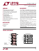

5
LT1039/LT1039-16
1039fd
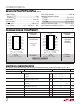
TYPICAL PERFORMANCE CHARACTERISTICS
U
W
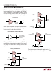
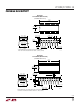
Shutdown to Receiver Output BIAS Pin Response Time
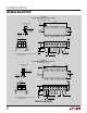
PIN FUNCTIONS
UUU
(Pin numbers listed are for 18-pin device)
V
+
, V
–
(Pins 1, 9): Driver Supply Pins. Supply current
drops to zero in shutdown mode. Driver outputs are in a
high impedance state when V
+
and V
–
= 0V.
BIAS (Pin 2): Keeps receiver 1 on while the LT1039 is in
the shutdown mode. Leave BIAS pin open when not in use.
See Applications Information for proper use.
REC IN (Pins 3, 5, 7): Receiver Input Pins. Accepts RS232
voltage levels (±30V) and has 0.4V of hysteresis to pro-
vide noise immunity. Input impedance is nominally 30kΩ.
TR OUT (Pins 4, 6, 8): Driver Outputs with RS232 Voltage
Levels. Outputs are in a high impedance state when in the
shutdown mode or when power is off (V
+
and V
–
= 0V) to
allow data line sharing. Outputs are fully short-circuit
protected from V
–
+ 30V to V
+
– 30V with power on, off or
in the shutdown mode. Typical output breakdowns are
greater than ±45V and higher applied voltages will not
damage the device if moderately current limited.
GND (Pin 10): Ground Pin.
TR IN (Pins 11, 13, 15): RS232 Driver Input Pins. Inputs
are TTL/CMOS compatible. Inputs should not be allowed
to float. Tie unused inputs to V
CC
.
REC OUT (Pins 12, 14, 16): Receiver Outputs with TTL/
CMOS Voltage Levels. Outputs are in a high impedance
state when in the shutdown mode to allow data line
sharing. Outputs are fully short-circuit protected to ground
or V
CC
with power on, off or in the shutdown mode.
ON/OFF (Pin 17): Controls the operation mode of the
LT1039 and is TTL/CMOS compatible. A logic low puts the
device in the shutdown mode which reduces input supply
current to zero and places both driver and receiver outputs
in a high impedance state.
V
CC
(Pin 18): 5V Power for Receivers.
6V
4V
2V
0V
RECEIVER
OUTPUT
5V
0V
ON/OFF
INPUT
1ms/DIV
1039 G11
V
CC
= 5V
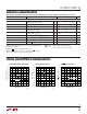
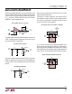
5V
BIAS INPUT
(THRU 25kΩ)
0.2µs/DIV
1039 G12
V
CC
= 5V
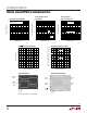
0V
2V
4V
6V
RECEIVER 1
OUTPUT
0V