
Datasheet

LT1073
5
OPERATIO
U
LT1073
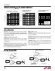
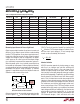
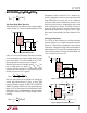
The LT1073 is gated oscillator switcher. This type archi-
tecture has very low supply current because the switch is
cycled only when the feedback pin voltage drops below the
reference voltage. Circuit operation can best be under-
stood by referring to the LT1073 Block Diagram. Com-
parator A1 compares the FB pin voltage with the 212mV
reference signal. When FB drops below 212mV, A1 switches
on the 19kHz oscillator. The driver amplifier boosts the
signal level to drive the output NPN power switch Q1. An
adaptive base drive circuit senses switch current and
provides just enough base drive to ensure switch satura-
tion without overdriving the switch, resulting in higher
efficiency. The switch cycling action raises the output
voltage and FB pin voltage. When the FB voltage is suffi-
cient to trip A1, the oscillator is gated off. A small amount
of hysteresis built into A1 ensures loop stability without
external frequency compensation. When the comparator
is low the oscillator and all high current circuitry is turned
off, lowering device quiescent current to just 95µA for the
reference, A1 and A2.
The oscillator is set internally for 38µs ON time and 15µs
OFF time, optimizing the device for step-up circuits where
V
OUT
≈ 3V
IN
, e.g., 1.5V to 5V. Other step-up ratios as well
as step-down (buck) converters are possible at slight
losses in maximum achievable power output.
A2 is a versatile gain block that can serve as a low-battery
detector, a linear post-regulator, or drive an undervoltage
lockout circuit. The negative input of A2 is internally
connected to the 212mV reference. An external resistor
divider from V
IN
to GND provides the trip point for A2. The
AO output can sink 100µA (use a 56k resistor pull-up to
5V). This line can signal a microcontroller that the battery
voltage has dropped below the preset level.
A resistor connected between the I
LIM
pin and V
IN
adjusts
maximum switch current. When the switch current ex-
ceeds the set value, the switch is turned off. This feature
is especially useful when small inductance values are used
with high input voltages. If the internal current limit of 1.5A
is desired, I
LIM
should be tied directly to V
IN
. Propagation
delay through the current-limit circuitry is about 2µs.
In step-up mode, SW2 is connected to ground and SW1
drives the inductor. In step-down mode, SW1 is con-
nected to V
IN
and SW2 drives the inductor. Output voltage
is set by the following equation in either step-up or step-
down modes where R1 is connected from FB to GND and
R2 is connected from V
OUT
to FB.
VmV
R
R
OUT
=
()
+
212
2
1
1
LT1073-5 and LT1073-12
The LT1073-5 and LT1073-12 fixed output voltage ver-
sions have the gain-setting resistor on-chip. Only three
external components are required to construct a fixed-
output converter. 5µA flows through R1 and R2 in the
LT1073-5, and 12.3µA flows in the LT1073-12. This
current represents a load and the converter must cycle
from time to time to maintain the proper output voltage.
Output ripple, inherently present in gated-oscillator de-
signs, will typically run around 150mV for the LT1073-5
and 350mV for the LT1073-12 with the proper inductor/
capacitor selection. This output ripple can be reduced
considerably by using the gain block amp as a preamplifier
in front of the FB pin. See the Applications Information
section for details.