
Datasheet


LT1074/LT1076
11
sn1074 1074fds
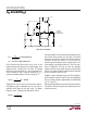
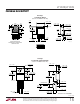
Figure 8. I
LIM
Pin Circuit
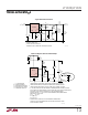
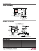
Figure 9. Foldback Current Limit
DESCRIPTIO S
U
PI
U
I
LIM
PIN
The I
LIM
pin is used to reduce current limit below the
preset value of 6.5A. The equivalent circuit for this pin is
shown in Figure 8.
Q1
R1
8K
TO LIMIT
CIRCUIT
V
IN
320 Aµ
D1
D3
6V
I
LIM
4.3V
D2
LT1047•PD12
When I
LIM
is left open, the voltage at Q1 base clamps at 5V
through D2. Internal current limit is determined by the
current through Q1. If an external resistor is connected
between I
LIM
and ground, the voltage at Q1 base can be
reduced for lower current limit. The resistor will have a
voltage across it equal to (320µA)(R), limited to ≈5V when
clamped by D2. Resistance required for a given current
limit is:
R
LIM
= I
LIM
(2kΩ) + 1kΩ (LT1074)
R
LIM
= I
LIM
(5.5kΩ) + 1kΩ (LT1076)
As an example, a 3A current limit would require
3A(2k) + 1k = 7kΩ for the LT1074. The accuracy of these
formulas is ±25% for 2A ≤ I
LIM
≤ 5A (LT1074) and
7A ≤ I
LIM
≤ 1.8A (LT1076), so I
LIM
should be set at least
25% above the
peak
switch current required.
Foldback current limiting can be easily implemented by
adding a resistor from the output to the I
LIM
pin as shown
in Figure 9. This allows full desired current limit (with or
without R
LIM
) when the output is regulating, but reduces
current limit under short-circuit conditions. A typical value
for R
FB
is 5kΩ, but this may be adjusted up or down to set
the amount of foldback. D2 prevents the output voltage
from forcing current back into the I
LIM
pin. To calculate a
value for R
FB
, first calculate R
LIM
, the R
FB
:
R
IR
Rk I
Rink
FB
SC L
LSC
L
=
−
()()
−Ω
()
−
Ω
()
044
05 1
.*
.*
*Change 0.44 to 0.16, and 0.5 to 0.18 for LT1076.
Example: I
LIM
= 4A, ISC = 1.5A, R
LIM
= (4)(2k) + 1k = 9k
R
k
kk
k
FB
=
−
()
Ω
()
−
()
−
Ω
()
15 044 9
059 1 15
38
..
..
.
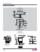
Error Amplifier
The error amplifier in Figure 10 is a single stage design
with added inverters to allow the output to swing above
and below the common mode input voltage. One side of
the amplifier is tied to a trimmed internal reference voltage
of 2.21V. The other input is brought out as the FB (feed-
back) pin. This amplifier has a G
M
(voltage “in” to current
“out”) transfer function of ≈5000µmho. Voltage gain is
determined by multiplying G
M
times the total equivalent
output loading, consisting of the output resistance of Q4
and Q6 in parallel with the series RC external frequency
compensation network. At DC, the external RC is ignored,
and with a parallel output impedance for Q4 and Q6 of
400kΩ, voltage gain is ≈2000. At frequencies above a few
hertz, voltage gain is determined by the external compen-
sation, R
C
and C
C
.
V
OUT
I
LIM
FB
R
LIM
R
FB
D2
1N4148
LT1074•PD13
LT1074