
Datasheet


4
LT1080/LT1081
10801fe
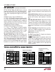
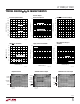
PI FU CTIO S
UUU
(Pin numbers refer to LT1080)
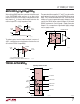
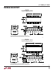
TEMPERATURE (°C)
–55 –25 0 25 50 75 100 125
DRIVER OUTPUT VOLTAGE (V)
1080/81 G01
10
8
6
4
2
0
–2
–4
–6
–8
–10
V
CC
= 5.5V
V
CC
= 4.5V
R
L
= 3k
OUTPUT HIGH
V
CC
= 5.5V
V
CC
= 4.5V
OUTPUT LOW
V
CC
= 5V
V
CC
= 5V
TIME (ms)
0 0.2 0.4 0.6 0.8 1.0 1.2 1.4 1.6 1.8 2.0
SUPPLY VOLTAGE (V)
1080/81 G03
10
8
6
4
2
0
–2
–4
–6
–8
–10
V
+
SUPPLY
V
CC
= 5V
C1 TO C4 = 1µF
R
L
= 4.7k; V
+
TO V
–
V
–
SUPPLY
OUTPUT CURRENT (mA)
02468101214161820
OUTPUT VOLTAGE (V)
1080/81 G02
10
8
6
4
2
0
–2
–4
–6
–8
–10
V
CC
= 5V
V
+
OUTPUT VOLTAGE
LOADED TO V
–
LOADED TO GROUND
LOADED TO GROUND
LOADED TO V
+
V
–
OUTPUT VOLTAGE
Driver Output Voltage Supply Generator Outputs
Supply Generation from V
CC
or Shutdown
C1
+
; C1
–
; C2
+
; C2
–
(Pins 2, 4, 5, 6): Requires an external
capacitor (≥1µF) from C1
+
to C1
–
and another from C2
+
to C2
–
. Pin 2 can be used for connecting a second positive
supply. When a separate positive supply is used, C1 can be
deleted.
V
+
(Pin 3): Positive Supply for RS232 Drivers.
V
+
≈ 2V
CC
– 1.5V. Requires an exterenal capacitor (≥1µF)
for charge storage. May be loaded (up to 15mA) for
external system use. Loading does reduce V
+
voltage (see
graphs). Capacitor may be tied to ground or +5V input
supply. With multiple transceivers, the V
+
and V
–
pins may
be paralleled into common capacitors.
V
–
(Pin 7): Negative Supply for RS232 Drivers.
V
–
≈ –(2V
CC
– 2.5V). Requires an external capacitor
(≥1µF) for charge stroage. May be loaded (up to –15mA)
for external system use. Loading does reduce V
–
voltage
(see graphs). With multiple transceivers, the V
+
and V
–
pins may be paralleled into common capacitors.
TR2 OUT; TR1 OUT (Pins 8, 15): Driver Outputs with
RS232 Voltage Levels. Outputs are in a high impedance
state when in the SHUTDOWN mode or when power is off
(V
CC
= 0V) to allow data line sharing. Outputs are fully
short-circuit protected from (V
–
+ 30V) to (V
+
– 30V) with
power on, off or in the SHUTDOWN mode. Typical output
breakdowns are greater than ±45V and higher applied
voltages will not damage the device if moderately current
limited. Shorting one output will affect output from the
other.
REC2 IN; REC1 IN (Pins 9, 14): Receiver Inputs. Accepts
RS232 voltage levels (±30V) and has 0.4V of hysteresis to
provide noise immunity. Input impedance is nominally
5kΩ.
REC2 OUT; REC1 OUT (Pins 10, 13): Receiver Outputs
with TTL/CMOS Voltage Levels. Outputs are in a high
impedance state when in the SHUTDOWN mode to allow
data line sharing. Outputs are fully short-circuit protected
to ground or V
CC
with power on, off or in the SHUTDOWN
mode.
TR2 IN; TR1 IN (Pins 11, 12): RS232 Driver Input Pins.
Inputs are TTL/CMOS compatible. Inputs should not be
allowed to float. Tie unused inputs to V
CC
.
GND (Pin 16): Ground Pin.
V
CC
(Pin 17): Input Supply Pin. Supply current drops to
zero in the SHUTDOWN mode.
ON/OFF (Pin 18): Contols the operation mode of the
LT1080 and is TTL/CMOS compatible. A logic low puts the
device in the SHUTDOWN mode which reduces input
supply current to zero and places both driver and receiver
outputs in a high impedance state. A logic high fully
enables the device.
TYPICAL PERFOR A CE CHARACTERISTICS
UW