
Datasheet

4
LT1083/84/85 Fixed
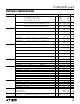
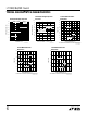
PARAMETER CONDITIONS MIN TYP MAX UNITS
Ripple Rejection LT1085-3.3 f = 120Hz, C
OUT
= 25µF Tantalum, V
IN
= 6.3V, I
OUT
= 3A ● 60 72 dB
LT1085-3.6 f = 120Hz, C
OUT
= 25µF Tantalum, V
IN
= 6.6V, I
OUT
= 3A ● 60 72 dB
LT1083/4/5-5 V
IN
= 8V (Note 5) ● 60 68 dB
LT1083/4/5-12 V
IN
= 15V (Note 5) ● 54 60 dB
Temperature Stability ● 0.5 %
Long Term Stability T
A
= 125°C, 1000 Hrs. 0.03 1.0 %
RMS Output Noise T
A
= 25°C,
(% of V
OUT
) 10Hz = ≤ f ≤ 10kHz 0.003 %
Thermal Resistance Control Circuitry/Power Transistor (See Applications Information)
Junctrion-to-Case LT1083 K Package 0.6/1.6 °C/W
P Package 0.5/1.6 °C/W
LT1084 K Package 0.75/2.3 °C/W
P Package 0.65/2.3 °C/W
T Package 0.65/2.7 °C/W
LT1085 K Package 0.9/3.0 °C/W
T Package 0.7/3.0 °C/W
DD Package 0.7/3.0 °C/W
ELECTRICAL CHARACTERISTICS
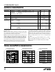
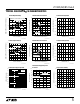
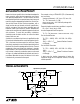
TYPICAL PERFORMANCE CHARACTERISTICS
U
W
input to output voltage. Note that the 60W power dissipation for the
LT1083 (45W for the LT1084 (K, P), 30W for the LT1084 (T), 30W for the
LT1085) is only achievable over a limited range of input to output voltage.
Note 4: Dropout voltage is specified over the full output current range of
the device. Test points and limits are shown on the Dropout Voltage curve.
Note 5: For LT1083 I
FULL LOAD
is 5A for –55°C ≤ T
J
≤ –40°C and 7.5A for
T
J
≥ –40°C.
Note 6: 1.7V ≤ (V
IN
– V
OUT
) ≤ 25V for LT1084 at –55°C ≤ T
J
≤ –40°C.
Note 7: Dropout voltage 1.7V maximum for LT1084 at –55 ≤ T
J
≤ –40°C.
Note 8: Full load current is not available at all input-output voltages.
See Notes 2,3,5.
OUTPUT CURRENT (A)
0
MINIMUM INPUT/OUTPUT DIFFERENTIAL (V)
1
2
LT1083/4/5 FIXED G01
0
12345678910
INDICATES GUARANTEED TEST POINT
–40°C ≤ T
J
≤ 150°C
0°C ≤ T
J
≤ 125°C
T
J
= 150°C
T
J
= 25°C
T
J
= –55°C
INPUT/OUTPUT DIFFERENTIAL (V)
0
SHORT-CIRCUIT CURRENT (A)
8
10
12
15 25
LT1083/4/5 FIXED G02
6
4
510
20 30 35
2
0
25°C
–55°C
I
FULL LOAD
GUARANTEED
150°C
TEMPERATURE (°C)
–50
–0.20
OUTPUT VOLTAGE DEVIATION (%)
–0.15
–0.10
–0.05
0
050
100
150
LT1083/4/5 FIXED G03
0.05
0.10
–25 25
75
125
∆I = 7.5A
LT1083 Dropout Voltage
LT1083 Load Regulation
LT1083 Short-Circuit Current
The ● denotes the specifications which apply over the full operating
temperature range.
Note 1: See thermal regulation specifications for changes in output voltage
due to heating effects. Load and line regulation are measured at a constant
junction temperature by low duty cycle pulse testing.
Note 2: Line and load regulation are guaranteed up to the maximum power
dissipation (60W for the LT1083, 45W for the LT1084 (K, P), 30W for the
LT1084 (T) and 30W for the LT1085). Power dissipation is determined by
the input/output differential and the output current. Guaranteed maximum
power dissipation will not be available over the full input/output range.
Note 3: I
FULL LOAD
is defined in the current limit curves. The I
FULLLOAD
curve is defined as the minimum value of current limit as a function of